Introductory Circuit Analysis (13th Edition)
Introductory Circuit Analysis (13th Edition)
13th Edition
ISBN: 9780133923605
Author: Robert L. Boylestad
Publisher: PEARSON
expand_more
expand_more
format_list_bulleted
Bartleby Related Questions Icon
Related questions
Question
NO AI. NEED EXPLANATION ALSO PLEASE
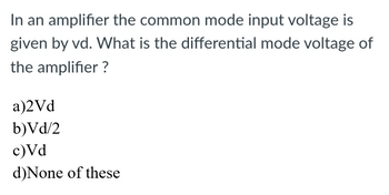
Transcribed Image Text:In an amplifier the common mode input voltage is
given by vd. What is the differential mode voltage of
the amplifier?
a)2Vd
b)Vd/2
c)Vd
d)None of these
Expert Solution
Check MarkThis question has been solved!
Explore an expertly crafted, step-by-step solution for a thorough understanding of key concepts.
bartleby
Step by stepSolved in 2 steps
Knowledge Booster
Background pattern image
Similar questions
- 6) Consider the following multistage amplifier. Draw the corresponding small signal model. Label, Vin, Vo1 and Vo. Do NOT make any approximations. Do NOT perform small signal analysis with this model. Just draw the small signal model. Show your work! Vin Vcc malli Q1 Re1 Vo1 Vcc ww1. Rc2 Q2 Re2 Voarrow_forwardThe figure below shows a direct coupled two-stage amplifier. Determine. (i) d.c. voltages for both stages (VB1, VB2, Vc1, Vc2, VE1 and VE2. voltage gain of each stage and overall voltage gain.arrow_forward4) Below is the small signal model of a multistage amplifier. Using this model, write the equationsthat you would need to determine the voltagegain. IMPORTANT: You only need to providethe equations that you would need to determinethe voltage gain. You DO NOT need to combine and simplify the equationsto determine a final expression for the voltagegain. Vin Vo Vb vo1 Rb R13 Vbe1 Vbe2 'e gm 1 Vbe1 gm 2 Vbe2 Rc2 Rc1 Rearrow_forward
- Q2: For the circuit shown in figure (2), he=100 for all transistors and 1/hobs = 200k2. Find: a. DC values for Ics, Ici. Vez, Ic7 and Vco. b. Ad, A, and CMRR of the difference amplifier. +15v 10KE 100k 1k 10k Q8 Q3 v1 Q7 25k Q1 Q2 14.3k Q5 Q6 Q9 -15v Figure (2)arrow_forwardII.The following figure shows a class AB amplifier. (a) Determine the parameters of dc VB (Q1), VB (Q2), VE, ICQ, VCEQ (Q1), VCEQ (Q2). (b) For a 5-Vrms input, determine the power that is provided to the load resistor, and (c) Draw the output signal +Vcc +9 V 1.0kn D: R 5.0 V rms R2 10 kN -Vecarrow_forwardFigure 4 shows a differential amplifier where the input voltage is Vin = Vil the output voltage is Vout - Vi2 and %3D Vo- (a) What kind of amplifier is it? Draw the small equivalent circuit and calculate the differential voltage gain G, in the case of balanced input and unbalanced output. For the calculation, consider the output resistances roi of the two transistors as open circuits (negligible current flowing in them). Show the detail of the calculation and state any assumption. (b) (c) What is Gv if you include the output resistances roi in the analysis? For the balanced input and identical transistors, the current variation in M1 and M2 are equal and opposite: i1 = -i2 (the current flowing in Rs is i- 0). V DD Rp1 Rp2 VinLM, M2 V2 V'ss =0 V Figure 4arrow_forward
- help with some explanationarrow_forward1) DC offsets, bias currents Vin R1 www 1k www Ú1 R3 R2 www 4k OUT ww11. U2 R4 1k OUT R5 ww 1k Vout The bias characteristics for both amplifiers are VDCoffset = 4mV I bias = 2μA I1 bias = 2μa a) Determine a value for resistor R3 such that the output voltage due to DC biases is zero.arrow_forwardQ1. Figure 1 shows a differential amplifier. Assume that all transistors are identical. 3=180, V2=0.026 Vand VBE = 0.7V. a) b) c) Show that the d.c. bias current to the differential pairs is Iccs = 0.6 m.A. Calculate the d.c. voltages at the output terminals V1 and 12 Given that the input signals are V1 = 4sin(wt) and V1 = 2 sin(wt) in mV, find the a.c. voltage between Vo1 and Vo2- 5k0 9.6k0 +12 V 6k0 200411 011 Figure 1 I CCS 12k0 6k0 0411arrow_forward
- Problem 3: The circuit below is a BJT common collector amplifier. Obtain expressions for both the voltage gain A, = You and the current gain A1 = put. Assume Vin » VBE. Vol (Power supply) To 2 Tin Ic 2 9m 2 Ic VT Rin B www. + vin -VBE RL B 1+3 V BE [te] IC VCE E Tout RL O Vin - VBE + Voutarrow_forwardA field effect transistor (FET) A. Uses a forward bias p-n junction, B. Uses a high concentration emitter junction, C. Has a very high input resistance, D. Depends on flow of minority carrier. As compared to transistor amplifier JFET amplifier has A. Higher voltage gain, less input impedance, B. Less voltage gain, less input impedance, C. Less voltage gain, higher input impedance, D. Higher voltage gain, higher input impedance. The pinch off voltage is the voltage A. At which gate source junction breaks down, B. Which causes depletion regions to meet, C. The voltage applied between drain & source, D. Neither of these. O If properly biased JFET acts as A. Current controlled current source, B. Voltage controlled voltage source, C. Voltage controlled current source, D. Current controlled voltage source.arrow_forwardDesign a circuit to simulate the following mathematical equation using minimum number of operational amplifiers. 5f Vout = 12V1 +5 V2 dt + 6 Where Vout is the output voltage, V1 and V2 are the input voltages. Assume that the available Dc source is +/- 5 volt.arrow_forward
arrow_back_ios
SEE MORE QUESTIONS
arrow_forward_ios
Recommended textbooks for you
- Text book imageIntroductory Circuit Analysis (13th Edition)Electrical EngineeringISBN:9780133923605Author:Robert L. BoylestadPublisher:PEARSONText book imageDelmar's Standard Textbook Of ElectricityElectrical EngineeringISBN:9781337900348Author:Stephen L. HermanPublisher:Cengage LearningText book imageProgrammable Logic ControllersElectrical EngineeringISBN:9780073373843Author:Frank D. PetruzellaPublisher:McGraw-Hill Education
- Text book imageFundamentals of Electric CircuitsElectrical EngineeringISBN:9780078028229Author:Charles K Alexander, Matthew SadikuPublisher:McGraw-Hill EducationText book imageElectric Circuits. (11th Edition)Electrical EngineeringISBN:9780134746968Author:James W. Nilsson, Susan RiedelPublisher:PEARSONText book imageEngineering ElectromagneticsElectrical EngineeringISBN:9780078028151Author:Hayt, William H. (william Hart), Jr, BUCK, John A.Publisher:Mcgraw-hill Education,
Text book image
Introductory Circuit Analysis (13th Edition)
Electrical Engineering
ISBN:9780133923605
Author:Robert L. Boylestad
Publisher:PEARSON
Text book image
Delmar's Standard Textbook Of Electricity
Electrical Engineering
ISBN:9781337900348
Author:Stephen L. Herman
Publisher:Cengage Learning
Text book image
Programmable Logic Controllers
Electrical Engineering
ISBN:9780073373843
Author:Frank D. Petruzella
Publisher:McGraw-Hill Education
Text book image
Fundamentals of Electric Circuits
Electrical Engineering
ISBN:9780078028229
Author:Charles K Alexander, Matthew Sadiku
Publisher:McGraw-Hill Education
Text book image
Electric Circuits. (11th Edition)
Electrical Engineering
ISBN:9780134746968
Author:James W. Nilsson, Susan Riedel
Publisher:PEARSON
Text book image
Engineering Electromagnetics
Electrical Engineering
ISBN:9780078028151
Author:Hayt, William H. (william Hart), Jr, BUCK, John A.
Publisher:Mcgraw-hill Education,