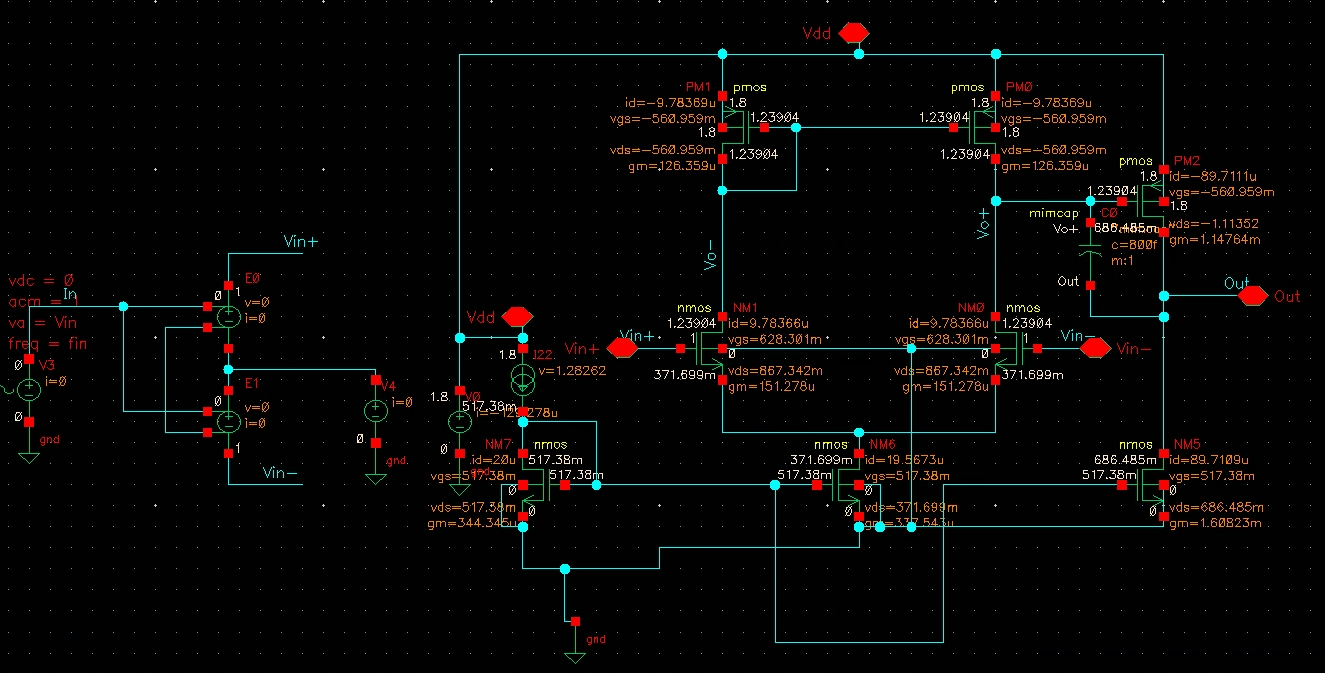
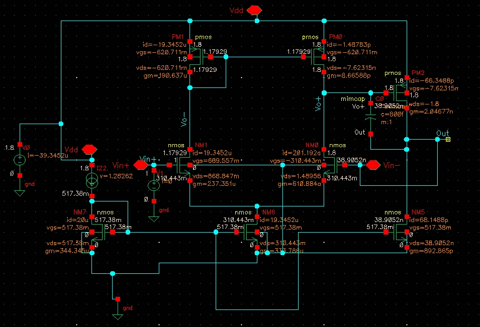
This is my first time designing an op amp, using 180nm in Cadence. Two stage design, 1st stage is NMOS differential pair with PMOS current mirror load, second stage is PMOS CS with Miller capacitor. Here's the DC operating points.
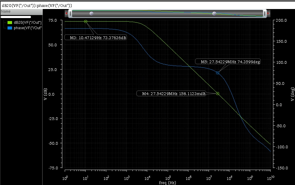
I have 1V common going into both inputs for the open loop. The current source is set to 20uA, the Vdd is 1.8V. Here's my open loop AC analysis.
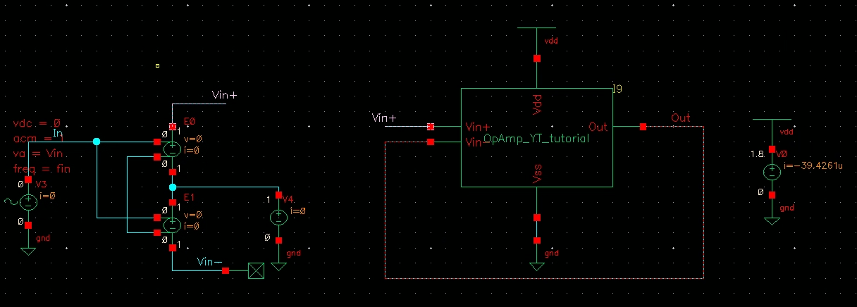
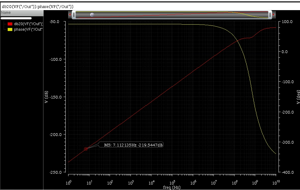
As you can see from the graph, the gain is 73dB in open loop, which should be high enough, and the gain margin is great. At DC, the output is nearly Vdd/2, so that should be okay. Now all I've done is connect the output back to the input as a unity buffer, which should give me a gain of 0dB or close to it, and instead I am getting baffling gains of -200dB or -400dB. The output seems to immediately saturate to one of the rails when I look at a transient simulation.
Am I just running the testbench wrong? It feels like it should be very simple and that I'm making some simulation mistake that's causing a convergence error or something in Cadence. Any insight or help appreciated, let me know if you need more details from me.
edit: DC operating point for closed loop gain enter image description here
-
\$\begingroup\$ Maybe it is oscillating due to phase shift. \$\endgroup\$Audioguru– Audioguru2021年12月12日 01:03:42 +00:00Commented Dec 12, 2021 at 1:03
-
\$\begingroup\$ How would that happen if the open loop has high gain margin and its in unity feedback? \$\endgroup\$Shredder– Shredder2021年12月12日 01:05:44 +00:00Commented Dec 12, 2021 at 1:05
-
3\$\begingroup\$ Can you show the op point (just like in the first image) but for the unity gain setup? I think your op amps inputs are reversed (Vin+ should be vin-) \$\endgroup\$Mike– Mike2021年12月12日 01:35:21 +00:00Commented Dec 12, 2021 at 1:35
-
\$\begingroup\$ Post edited with closed loop DC operating point. The inputs should be correct, virtually every example I've seen has it this way. The positive input on one side becomes the positive output on the other of a diff pair, and then that single ended output becomes the CS stage input. \$\endgroup\$Shredder– Shredder2021年12月12日 01:48:28 +00:00Commented Dec 12, 2021 at 1:48
-
1\$\begingroup\$ Wait actually I think you're right. The positive output of the diff pair is then inverted by the CS stage, so what used to be the positive input of the differential pair is now the negative input? Is that correct? \$\endgroup\$Shredder– Shredder2021年12月12日 02:02:28 +00:00Commented Dec 12, 2021 at 2:02
1 Answer 1
Your open loop gain has a phase of -180 deg. Your VIN+ and VIN- labels are reversed.
This is not a good way to measure AC open loop gain; in general you can't get a good bias point, although it seems to work here. You need to close the loop DC, while open it AC. This is generally done with an extremely large inductor/capacitor arrangement. It is also possible to use a SPICE resistor if you can set different values for .AC and .DC (.OP) analyses.
-
\$\begingroup\$ Yup you got it. Completely missed my mind that the CS stage inverts the differential pair output so in fact I was creating a positive feedback loop. \$\endgroup\$Shredder– Shredder2021年12月12日 02:31:13 +00:00Commented Dec 12, 2021 at 2:31