Unusual circuits in the Intel 386's standard cell logic
I've been studying the standard cell circuitry in the Intel 386 processor recently. The 386, introduced in 1985, was Intel's most complex processor at the time, containing 285,000 transistors. Intel's existing design techniques couldn't handle this complexity and the chip began to fall behind schedule. To meet the schedule, the 386 team started using a technique called standard cell logic. Instead of laying out each transistor manually, the layout process was performed by a computer.
The idea behind standard cell logic is to create standardized circuits (standard cells) for each type of logic element, such as an inverter, NAND gate, or latch. You feed your circuit description into software that selects the necessary cells, positions these cells into columns, and then routes the wiring between the cells. This "automatic place and route" process creates the chip layout much faster than manual layout. However, switching to standard cells was a risky decision since if the software couldn't create a dense enough layout, the chip couldn't be manufactured. But in the end, the 386 finished ahead of schedule, an almost unheard-of accomplishment.1
The 386's standard cell circuitry contains a few circuits that I didn't expect. In this blog post, I'll take a quick look at some of these circuits: surprisingly large multiplexers, a transistor that doesn't fit into the standard cell layout, and inverters that turned out not to be inverters. (If you want more background on standard cells in the 386, see my earlier post, "Reverse engineering standard cell logic in the Intel 386 processor".)
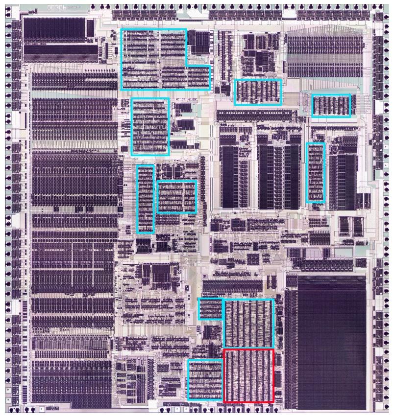
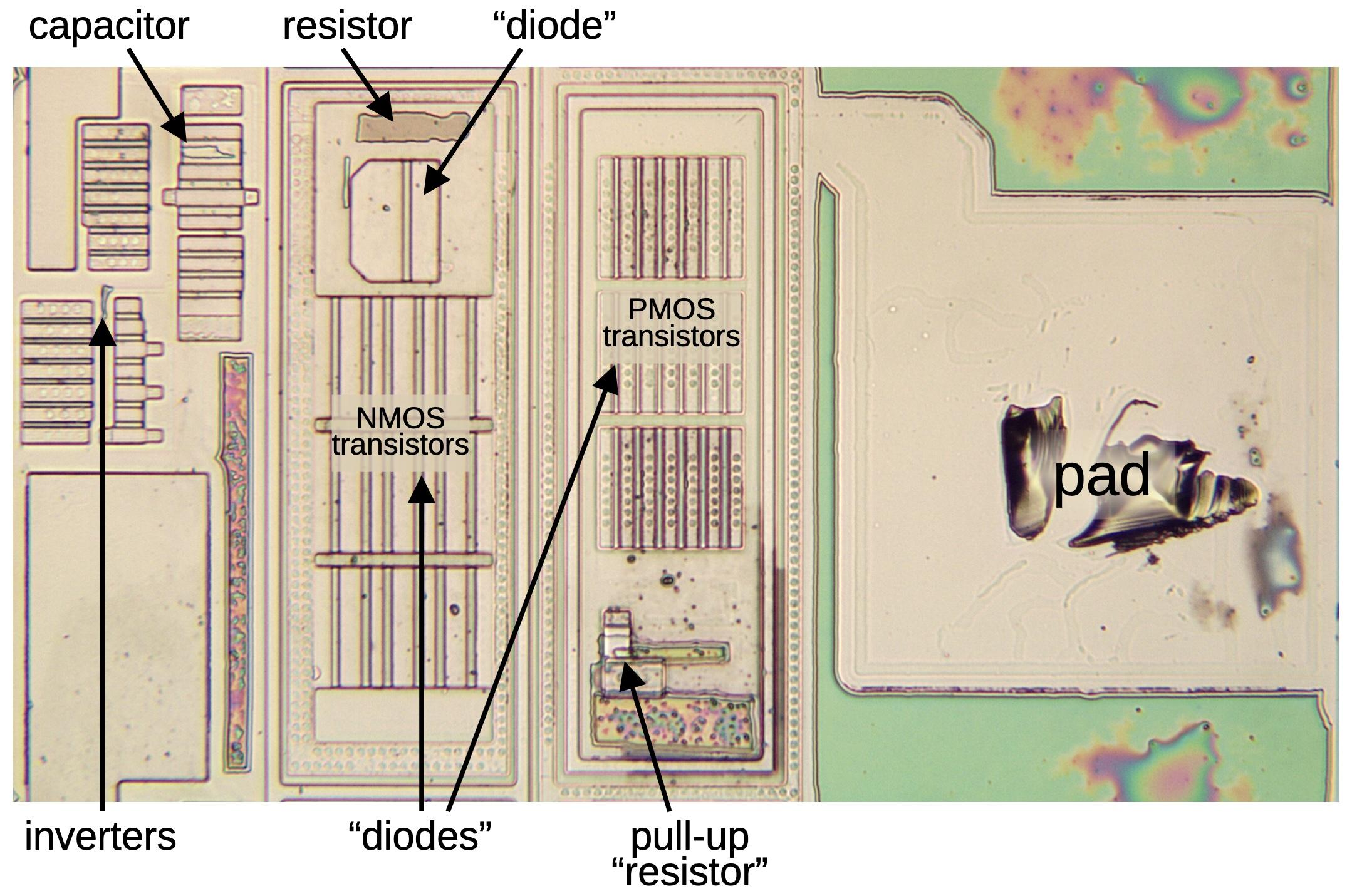
The photo below shows the 386 die with the automatic-place-and-route regions highlighted; I'm focusing on the red region in the lower right. These blocks of logic have cells arranged in rows, giving them a characteristic striped appearance. The dark stripes are the transistors that make up the logic gates, while the lighter regions between the stripes are the "routing channels" that hold the wiring that connects the cells. In comparison, functional blocks such as the datapath on the left and the microcode ROM in the lower right were designed manually to optimize density and performance, giving them a more solid appearance.
The 386 die with the standard-cell regions highlighted.
As for other features on the chip, the black circles around the border are bond wire connections that go to the chip's external pins. The chip has two metal layers, a small number by modern standards, but a jump from the single metal layer of earlier processors such as the 286. (Providing two layers of metal made automated routing practical: one layer can hold horizontal wires while the other layer can hold vertical wires.) The metal appears white in larger areas, but purplish where circuitry underneath roughens its surface. The underlying silicon and the polysilicon wiring are obscured by the metal layers.
The giant multiplexers
The standard cell circuitry that I'm examining (red box above) is part of the control logic that selects registers while executing an instruction. You might think that it is easy to select which registers take part in an instruction, but due to the complexity of the x86 architecture, it is more difficult. One problem is that a 32-bit register such as EAX can also be treated as the 16-bit register AX, or two 8-bit registers AH and AL. A second problem is that some instructions include a "direction" bit that switches the source and destination registers. Moreover, sometimes the register is specified by bits in the instruction, but in other cases, the register is specified by the microcode. Due to these factors, selecting the registers for an operation is a complicated process with many cases, using control bits from the instruction, from the microcode, and from other sources.
Three registers need to be selected for an operation—two source registers and a destination register—and there are about 17 cases that need to be handled. Registers are specified with 7-bit control signals that select one of the 30 registers and control which part of the register is accessed. With three control signals, each 7 bits wide, and about 17 cases for each, you can see that the register control logic is large and complicated. (I wrote more about the 386's registers here.)
I'm still reverse engineering the register control logic, so I won't go into details. Instead, I'll discuss how the register control circuit uses multiplexers, implemented with standard cells. A multiplexer is a circuit that combines multiple input signals into a single output by selecting one of the inputs.2 A multiplexer can be implemented with logic gates, for instance, by ANDing each input with the corresponding control line, and then ORing the results together. However, the 386 uses a different approach—CMOS switches—that avoids a large AND/OR gate.
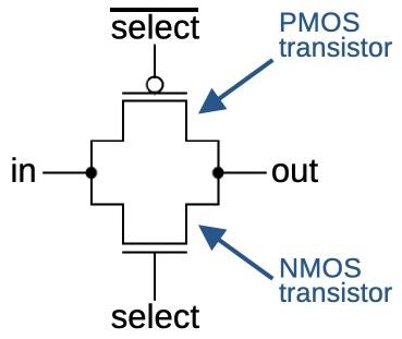
The schematic above shows how a CMOS switch is constructed from two MOS transistors. When the two transistors are on, the output is connected to the input, but when the two transistors are off, the output is isolated. An NMOS transistor is turned on when its input is high, but a PMOS transistor is turned on when its input is low. Thus, the switch uses two control inputs, one inverted. The motivation for using two transistors is that an NMOS transistor is better at pulling the output low, while a PMOS transistor is better at pulling the output high, so combining them yields the best performance.3 Unlike a logic gate, the CMOS switch has no amplification, so a signal is weakened as it passes through the switch. As will be seen below, inverters can be used to amplify the signal.
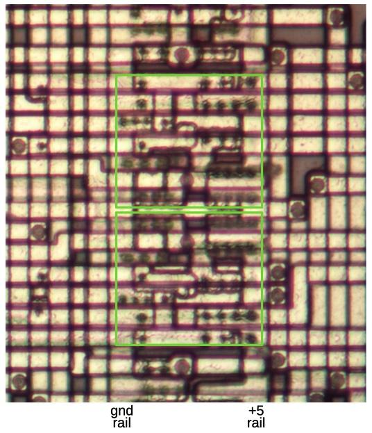
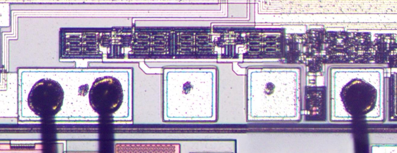
The image below shows how CMOS switches appear under the microscope. This image is very hard to interpret because the two layers of metal on the 386 are packed together densely, but you can see that some wires run horizontally and others run vertically. The bottom layer of metal (called M1) runs vertically in the routing area, as well as providing internal wiring for a cell. The top layer of metal (M2) runs horizontally; unlike M1, the M2 wires can cross a cell. The large circles are vias that connect the M1 and M2 layers, while the small circles are connections between M1 and polysilicon or M1 and silicon. The central third of the image is a column of standard cells with two CMOS switches outlined in green. The cells are bordered by the vertical ground rail and +5V rail that power the cells. The routing areas are on either side of the cells, holding the wiring that connects the cells.
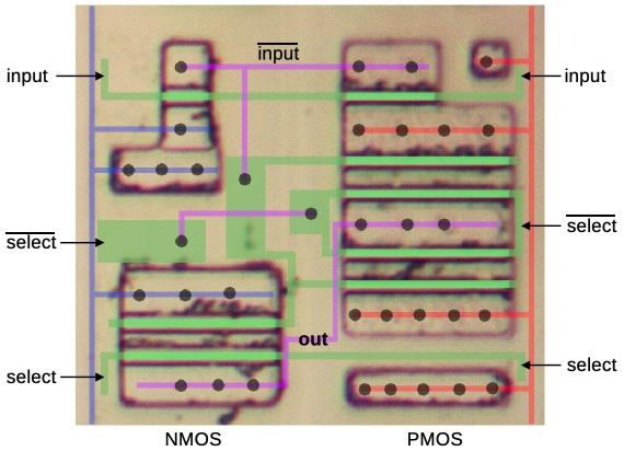
Removing the metal layers reveals the underlying silicon with a layer of polysilicon wiring on top. The doped silicon regions show up as dark outlines. I've drawn the polysilicon in green; it forms a transistor (brighter green) when it crosses doped silicon. The metal ground and power lines are shown in blue and red, respectively, with other metal wiring in purple. The black dots are vias between layers. Note how metal wiring (purple) and polysilicon wiring (green) are combined to route signals within the cell. Although this standard cell is complicated, the important thing is that it only needs to be designed once. The standard cells for different functions are all designed to have the same width, so the cells can be arranged in columns, snapped together like Lego bricks.
To summarize, this switch circuit allows the input to be connected to the output or disconnected, controlled by the select signal. This switch is more complicated than the earlier schematic because it includes two inverters to amplify the signal. The data input and the two select lines are connected to the polysilicon (green); the cell is designed so these connections can be made on either side. At the top, the input goes through a standard two-transistor inverter. The lower left has two transistors, combining the NMOS half of an inverter with the NMOS half of the switch. A similar circuit on the right combines the PMOS part of an inverter and switch. However, because PMOS transistors are weaker, this part of the circuit is duplicated.
A multiplexer is constructed by combining multiple switches, one for each input. Turning on one switch will select the corresponding input. For instance, a four-to-one multiplexer has four switches, so it can select one of the four inputs.
A four-way multiplexer constructed from CMOS switches and individual transistors.
The schematic above shows a hypothetical multiplexer with four inputs. One optimization is that if an input is always 0, the PMOS transistor can be omitted. Likewise, if an input is always 1, the NMOS transistor can be omitted. One set of select lines is activated at a time to select the corresponding input. The pink circuit selects 1, green selects input A, yellow selects input B, and blue selects 0. The multiplexers in the 386 are similar, but have more inputs.
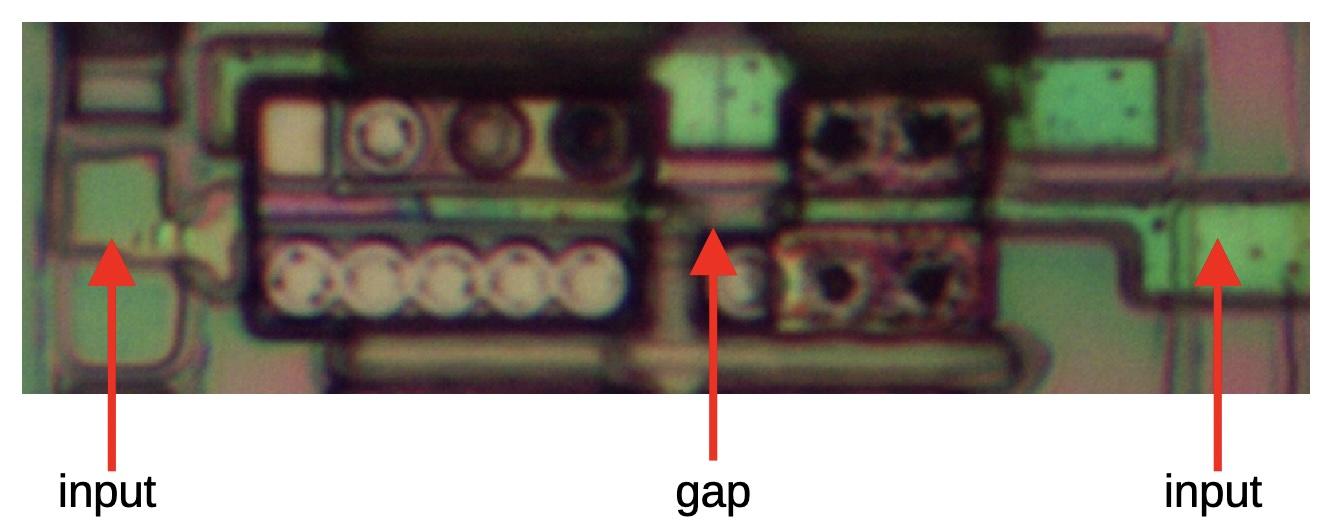
The diagram below shows how much circuitry is devoted to multiplexers in this block of standard cells. The green, purple, and red cells correspond to the multiplexers driving the three register control outputs. The yellow cells are inverters that generate the inverted control signals for the CMOS switches. This diagram also shows how the automatic layout of cells results in a layout that appears random.
The misplaced transistor
The idea of standard-cell logic is that standardized cells are arranged in columns. The space between the cells is the "routing channel", holding the wiring that links the cells. The 386 circuitry follows this layout, except for one single transistor, sitting between two columns of cells.
I wrote some software tools to help me analyze the standard cells. Unfortunately, my tools assumed that all the cells were in columns, so this one wayward transistor caused me considerable inconvenience.
The transistor turns out to be a PMOS transistor, pulling a signal high as part of a multiplexer. But why is this transistor out of place? My hypothesis is that the transistor is a bug fix. Regenerating the cell layout was very costly, taking many hours on an IBM mainframe computer. Presumably, someone found that they could just stick the necessary transistor into an unused spot in the routing channel, manually add the necessary wiring, and avoid the delay of regenerating all the cells.
The fake inverter
The simplest CMOS gate is the inverter, with an NMOS transistor to pull the output low and a PMOS transistor to pull the output high. The standard cell circuitry that I examined contains over a hundred inverters of various sizes. (Performance is improved by using inverters that aren't too small but also aren't larger than necessary for a particular circuit. Thus, the standard cell library includes inverters of multiple sizes.)
The image below shows a medium-sized standard-cell inverter under the microscope. For this image, I removed the two metal layers with acid to show the underlying polysilicon (bright green) and silicon (gray). The quality of this image is poor—it is difficult to remove the metal without destroying the polysilicon—but the diagram below should clarify the circuit. The inverter has two transistors: a PMOS transistor connected to +5 volts to pull the output high when the input is 0, and an NMOS transistor connected to ground to pull the output low when the input is 1. (The PMOS transistor needs to be larger because PMOS transistors don't function as well as NMOS transistors due to silicon physics.)
An inverter as seen on the die. The corresponding standard cell is shown below.
The polysilicon input line plays a key role: where it crosses the doped silicon, a transistor gate is formed. To make the standard cell more flexible, the input to the inverter can be connected on either the left or the right; in this case, the input is connected on the right and there is no connection on the left. The inverter's output can be taken from the polysilicon on the upper left or the right, but in this case, it is taken from the upper metal layer (not shown). The power, ground, and output lines are in the lower metal layer, which I have represented by the thin red, blue, and yellow lines. The black circles are connections between the metal layer and the underlying silicon.
This inverter appears dozens of times in the circuitry. However, I came across a few inverters that didn't make sense. The problem was that the inverter's output was connected to the output of a multiplexer. Since an inverter is either on or off, its value would clobber the output of the multiplexer.4 This didn't make any sense. I double- and triple-checked the wiring to make sure I hadn't messed up. After more investigation, I found another problem: the input to a "bad" inverter didn't make sense either. The input consisted of two signals shorted together, which doesn't work.
Finally, I realized what was going on. A "bad inverter" has the exact silicon layout of an inverter, but it wasn't an inverter: it was independent NMOS and PMOS transistors with separate inputs. Now it all made sense. With two inputs, the input signals were independent, not shorted together. And since the transistors were controlled separately, the NMOS transistor could pull the output low in some circumstances, the PMOS transistor could pull the output high in other circumstances, or both transistors could be off, allowing the multiplexer's output to be used undisturbed. In other words, the "inverter" was just two more cases for the multiplexer.
The "bad" inverter. (Image is flipped vertically for comparison with the previous inverter.)
If you compare the "bad inverter" cell below with the previous cell, they look almost the same, but there are subtle differences. First, the gates of the two transistors are connected in the real inverter, but disconnected by a small gap in the transistor pair. I've indicated this gap in the photo above; it is hard to tell if the gap is real or just an imaging artifact, so I didn't spot it. The second difference is that the "fake" inverter has two input connections, one to each transistor, while the inverter has a single input connection. Unfortunately, I assumed that the two connections were just a trick to route the signal across the inverter without requiring an extra wire. In total, this cell was used 32 times as a real inverter and 9 times as independent transistors.
Conclusions
Standard cell logic and automatic place and route have a long history before the 386, back to the early 1970s, so this isn't an Intel invention.5 Nonetheless, the 386 team deserves the credit for deciding to use this technology at a time when it was a risky decision. They needed to develop custom software for their placing and routing needs, so this wasn't a trivial undertaking. This choice paid off and they completed the 386 ahead of schedule. The 386 ended up being a huge success for Intel, moving the x86 architecture to 32 bits and defining the dominant computer architecture for the rest of the 20th century.
If you're interested in standard cell logic, I also wrote about standard cell logic in an IBM chip. I plan to write more about the 386, so follow me on Mastodon, Bluesky, or RSS for updates. Thanks to Pat Gelsinger and Roxanne Koester for providing helpful papers.
For more on the 386 and other chips, follow me on Mastodon (@[email protected]), Bluesky (@righto.com), or RSS. (I've given up on Twitter.) If you want to read more about the 386, I've written about the clock pin, prefetch queue, die versions, packaging, and I/O circuits.
Notes and references
-
The decision to use automatic place and route is described on page 13 of the Intel 386 Microprocessor Design and Development Oral History Panel, a very interesting document on the 386 with discussion from some of the people involved in its development. ↩
-
Multiplexers often take a binary control signal to select the desired input. For instance, an 8-to-1 multiplexer selects one of 8 inputs, so a 3-bit control signal can specify the desired input. The 386's multiplexers use a different approach with one control signal per input. One of the 8 control signals is activated to select the desired input. This approach is called a "one-hot encoding" since one control line is activated (hot) at a time. ↩
-
Some chips, such as the MOS Technology 6502 processor, are built with NMOS technology, without PMOS transistors. Multiplexers in the 6502 use a single NMOS transistor, rather than the two transistors in the CMOS switch. However, the performance of the switch is worse. ↩
-
One very common circuit in the 386 is a latch constructed from an inverter loop and a switch/multiplexer. The inverter's output and the switch's output are connected together. The trick, however, is that the inverter is constructed from special weak transistors. When the switch is disabled, the inverter's weak output is sufficient to drive the loop. But to write a value into the latch, the switch is enabled and its output overpowers the weak inverter.
The point of this is that there are circuits where an inverter and a multiplexer have their outputs connected. However, the inverter must be constructed with special weak transistors, which is not the situation that I'm discussing. ↩
-
I'll provide more history on standard cells in this footnote. RCA patented a bipolar standard cell in 1971, but this was a fixed arrangement of transistors and resistors, more of a gate array than a modern standard cell. Bell Labs researched standard cell layout techniques in the early 1970s, calling them Polycells, including a 1973 paper by Brian Kernighan. By 1979, A Guide to LSI Implementation discussed the standard cell approach and it was described as well-known in this patent application. Even so, Electronics called these design methods "futuristic" in 1980.
Standard cells became popular in the mid-1980s as faster computers and improved design software made it practical to produce semi-custom designs that used standard cells. Standard cells made it to the cover of Digital Design in August 1985, and the article inside described numerous vendors and products. Companies like Zymos and VLSI Technology (VTI) focused on standard cells. Traditional companies such as Texas Instruments, NCR, GE/RCA, Fairchild, Harris, ITT, and Thomson introduced lines of standard cell products in the mid-1980s. ↩
A Navajo weaving of an integrated circuit: the 555 timer
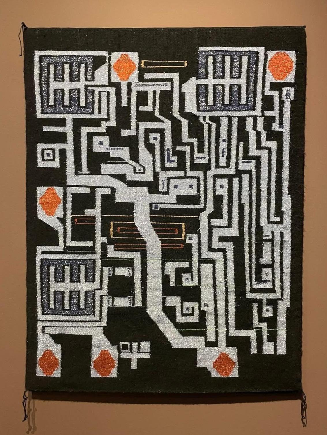
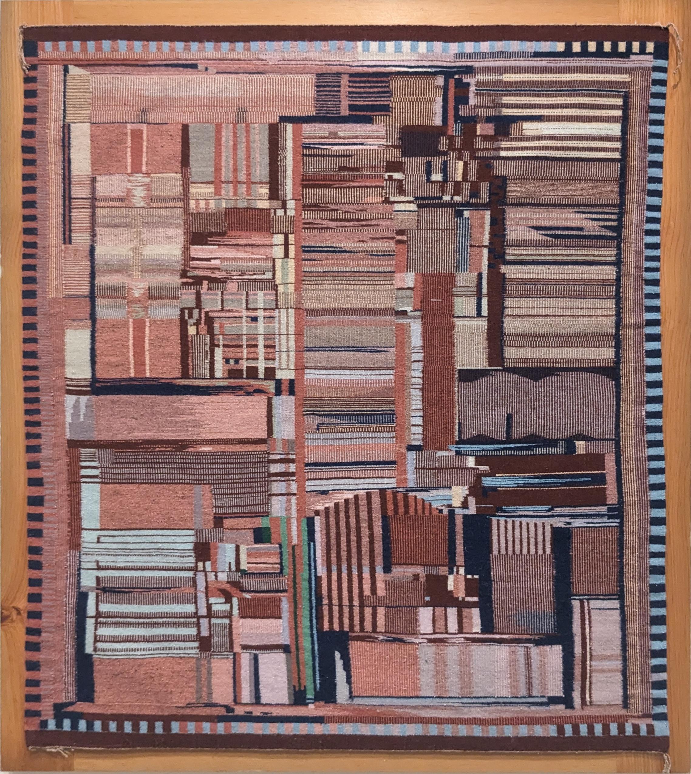
The noted Diné (Navajo) weaver Marilou Schultz recently completed an intricate weaving composed of thick white lines on a black background, punctuated with reddish-orange diamonds. Although this striking rug may appear abstract, it shows the internal circuitry of a tiny silicon chip known as the 555 timer. This chip has hundreds of applications in everything from a sound generator to a windshield wiper controller. At one point, the 555 was the world's best-selling integrated circuit with billions sold. But how did the chip get turned into a rug?
"Popular Chip" by Marilou Schultz. Photo courtesy of First American Art Magazine.
The 555 chip is constructed from a tiny flake of silicon with a layer of metallic wiring on top. In the rug, this wiring is visible as the thick white lines, while the silicon forms the black background. One conspicuous feature of the rug is the reddish-orange diamonds around the perimeter. These correspond to the connections between the silicon chip and its eight pins. Tiny golden bond wires—thinner than a human hair—are attached to the square bond pads to provide these connections. The circuitry of the 555 chip contains 25 transistors, silicon devices that can switch on and off. The rug is dominated by three large transistors, the filled squares with a 王 pattern inside, while the remaining transistors are represented by small dots.
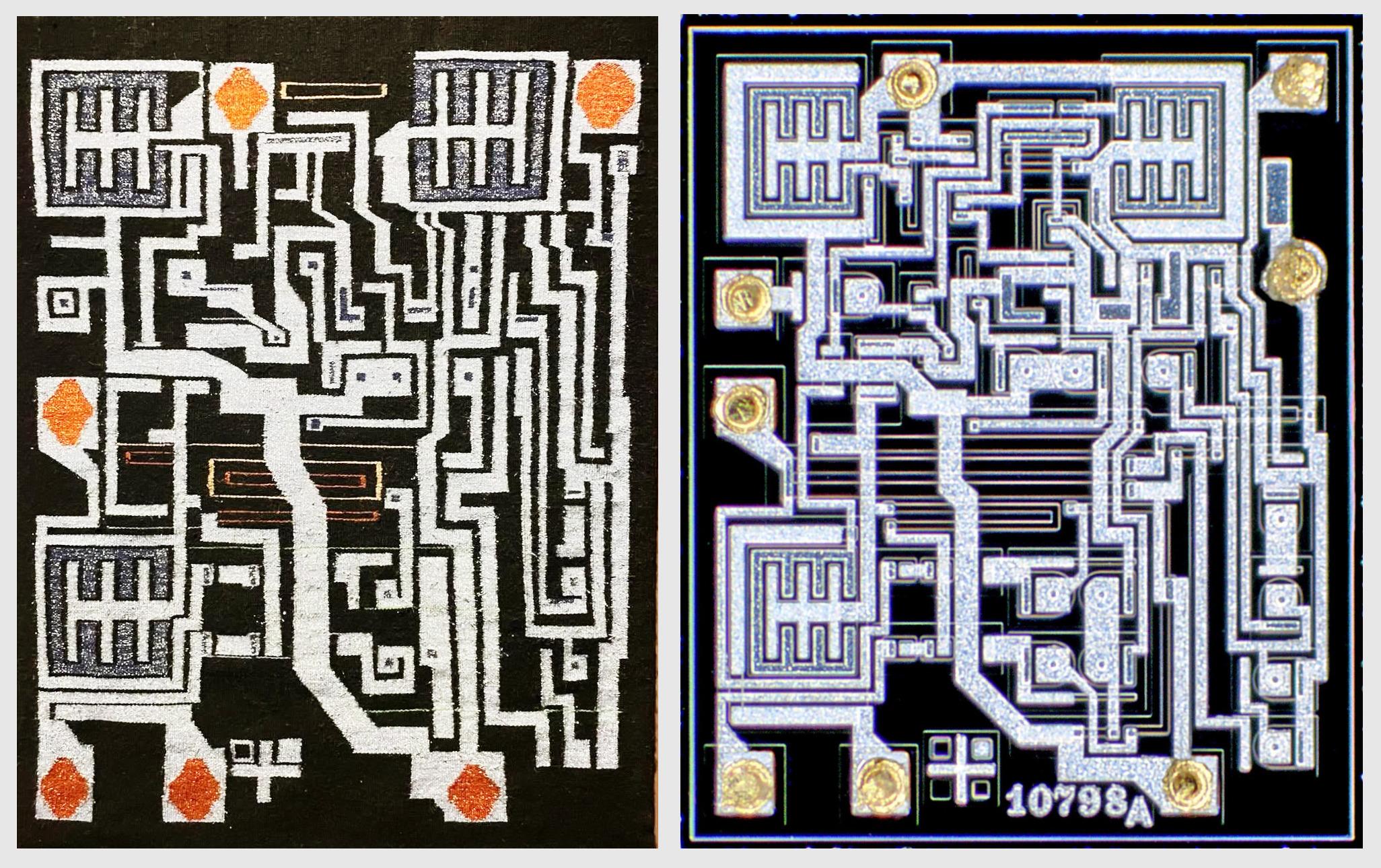
The weaving was inspired by a photo of the 555 timer die taken by Antoine Bercovici (Siliconinsider); I suggested this photo to Schultz as a possible subject for a rug. The diagram below compares the weaving (left) with the die photo (right). As you can see, the weaving closely follows the actual chip, but there are a few artistic differences. For instance, two of the bond pads have been removed, the circuitry at the top has been simplified, and the part number at the bottom has been removed.
Antoine took the die photo with a dark field microscope, a special type of microscope that produces an image on a black background. This image emphasizes the metal layer on the top of the die. In comparison, a standard bright-field microscope produced the image below. When a chip is manufactured, regions of silicon are "doped" with impurities to create transistors and resistors. These regions are visible in the image below as subtle changes in the color of the silicon.
The RCA CA555 chip. Photo courtesy of Tiny Transistors.
In the weaving, the chip's design appears almost monumental, making it easy to forget that the actual chip is microscopic. For the photo below, I obtained a version of the chip packaged in a metal can, rather than the typical rectangle of black plastic. Cutting the top off the metal can reveals the tiny chip inside, with eight gold bond wires connecting the die to the pins of the package. If you zoom in on the photo, you may recognize the three large transistors that dominate the rug.
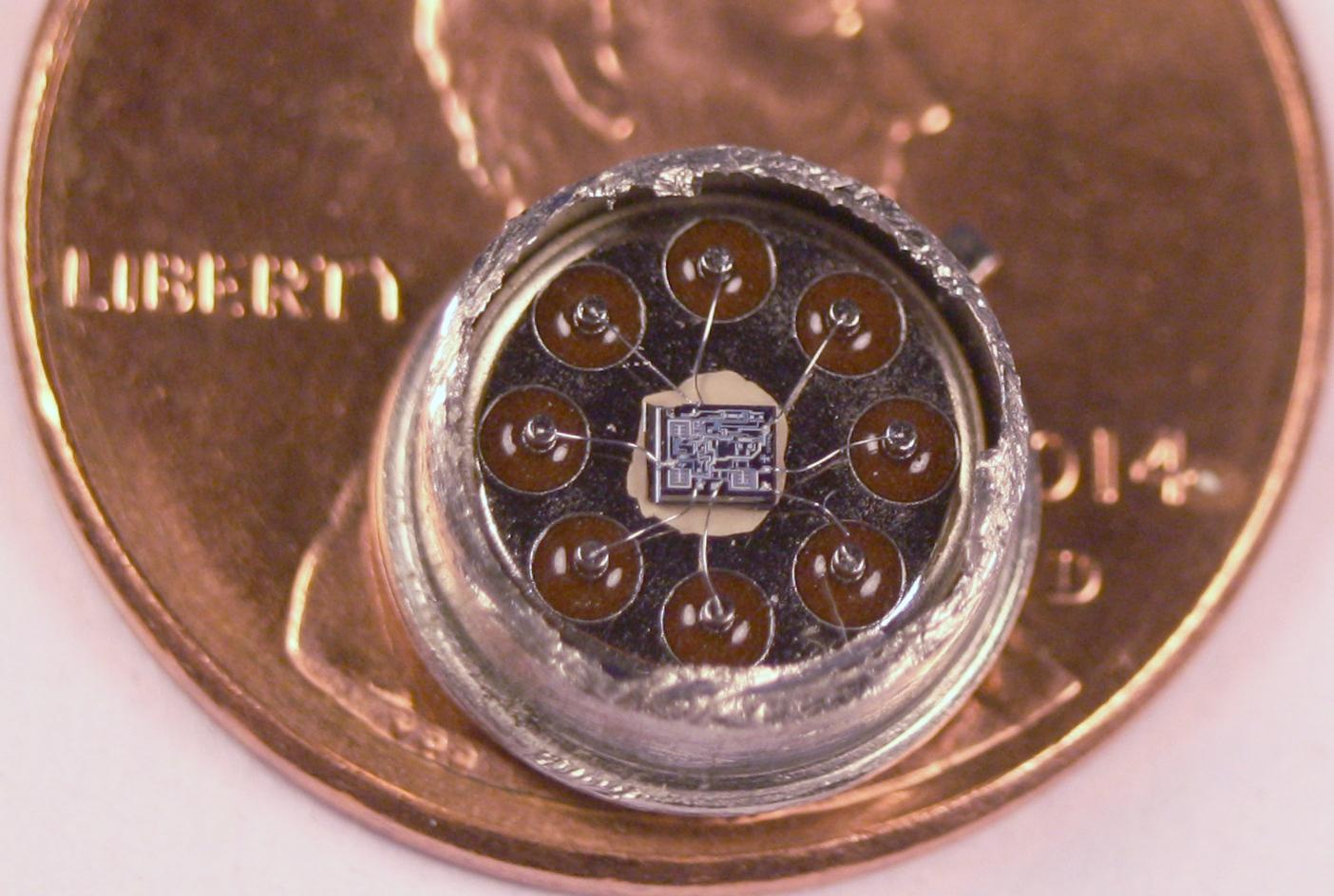
The artist, Marilou Schultz, has been creating chip rugs since 1994, when Intel commissioned a rug based on the Pentium as a gift to AISES (American Indian Science & Engineering Society). Although Schultz learned weaving as a child, the Pentium rug was a challenge due to its complex pattern and lack of symmetry; a day's work might add just an inch to the rug. This dramatic weaving was created with wool from the long-horned Navajo-Churro sheep, colored with traditional plant dyes.
For the 555 timer weaving, Schultz experimented with different materials. Silver and gold metallic threads represent the aluminum and copper in the chip. The artist explains that "it took a lot more time to incorporate the metallic threads," but it was worth the effort because "it is spectacular to see the rug with the metallics in the dark with a little light hitting it." Aniline dyes provided the black and lavender colors. Although natural logwood dye produces a beautiful purple, it fades over time, so Schultz used an aniline dye instead. The lavender colors are dedicated to the weaver's mother, who passed away in February; purple was her favorite color.
Inside the chip
How does the 555 chip produce a particular time delay? You add external components—resistors and a capacitor—to select the time. The capacitor is filled (charged) at a speed controlled by the resistor. When the capacitor get "full", the 555 chip switches operation and starts emptying (discharging) the capacitor. It's like filling a sink: if you have a large sink (capacitor) and a trickle of water (large resistor), the sink fills slowly. But if you have a small sink (capacitor) and a lot of water (small resistor), the sink fills quickly. By using different resistors and capacitors, the 555 timer can provide time intervals from microseconds to hours.
I've constructed an interactive chip browser that shows how the regions of the rug correspond to specific electronic components in the physical chip. Click on any part of the rug to learn the function of the corresponding component in the chip.
For instance, two of the large square transistors turn the chip's output on or off, while the third large transistor discharges the capacitor when it is full. (To be precise, the capacitor goes between 1/3 full and 2/3 full to avoid issues near "empty" and "full".) The chip has circuits called comparators that detect when the capacitor's voltage reaches 1/3 or 2/3, switching between emptying and filling at those points. If you want more technical details about the 555 chip, see my previous articles: an early 555 chip, a 555 timer similar to the rug, and a more modern CMOS version of the 555.
Conclusions
The similarities between Navajo weavings and the patterns in integrated circuits have long been recognized. Marilou Schultz's weavings of integrated circuits make these visual metaphors into concrete works of art. This connection is not just metaphorical, however; in the 1960s, the semiconductor company Fairchild employed numerous Navajo workers to assemble chips in Shiprock, New Mexico. I wrote about this complicated history in The Pentium as a Navajo Weaving.
This work is being shown at SITE Santa Fe's Once Within a Time exhibition (running until January 2026). I haven't seen the exhibition in person, so let me know if you visit it. For more about Marilou Schultz's art, see The Diné Weaver Who Turns Microchips Into Art, or A Conversation with Marilou Schultz on YouTube.
Many thanks to Marilou Schultz for discussing her art with me. Thanks to First American Art Magazine for providing the photo of her 555 rug. Follow me on Mastodon (@[email protected]), Bluesky (@righto.com), or RSS for updates.
Here be dragons: Preventing static damage, latchup, and metastability in the 386
I've been reverse-engineering the Intel 386 processor (from 1985), and I've come across some interesting circuits for the chip's input/output (I/O) pins. Since these pins communicate with the outside world, they face special dangers: static electricity and latchup can destroy the chip, while metastability can cause serious malfunctions. These I/O circuits are completely different from the logic circuits in the 386, and I've come across a previously-undescribed flip-flop circuit, so I'm venturing into uncharted territory. In this article, I take a close look at how the I/O circuitry protects the 386 from the "dragons" that can destroy it.
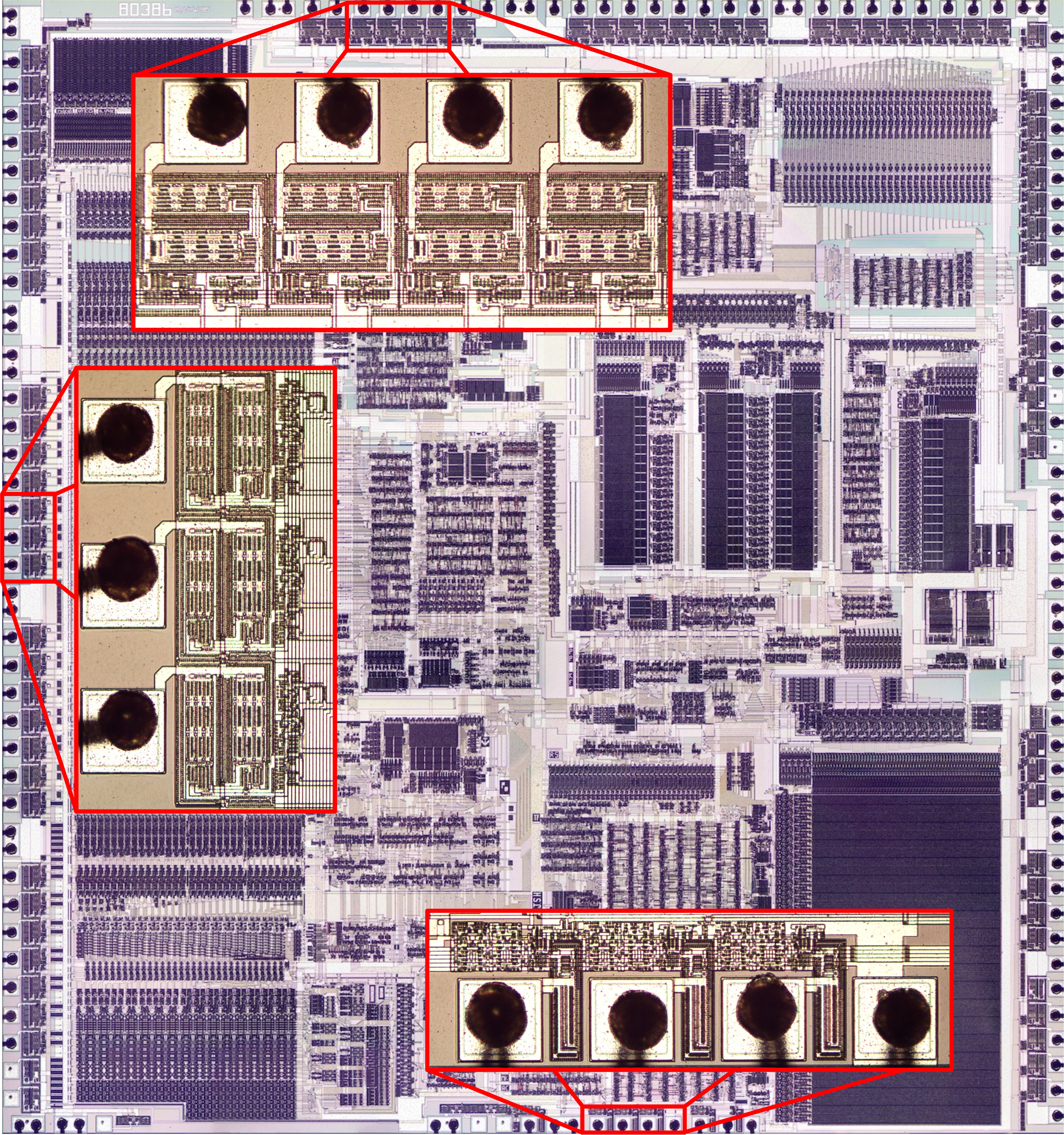
The photo above shows the die of the 386 under a microscope. The dark, complex patterns arranged in rectangular regions arise from the two layers of metal that connect the circuits on the 386 chip. Not visible are the transistors, formed from silicon and polysilicon and hidden beneath the metal. Around the perimeter of this fingernail-sized silicon die, 141 square bond pads provide the connections between the chip and the outside world; tiny gold bond wires connect the bond pads to the package. Next to each I/O pad, specialized circuitry provides the electrical interface between the chip and the external components while protecting the chip. I've zoomed in on three groups of these bond pads along with the associated I/O circuits. The circuits at the top (for data pins) and the left (for address pins) are completely different from the control pin circuits at the bottom, showing how the circuitry varies with the pin's function.
Static electricity
The first dragon that threatens the 386 is static electricity, able to burn a hole in the chip. MOS transistors are constructed with a thin insulating oxide layer underneath the transistor's gate. In the 386, this fragile, glass-like oxide layer is just 250 nm thick, the thickness of a virus. Static electricity, even a small amount, can blow a hole through this oxide layer and destroy the chip. If you've ever walked across a carpet and felt a spark when you touch a doorknob, you've generated at least 3000 volts of chip-destroying static electricity. Intel recommends an anti-static mat and a grounding wrist strap when installing a processor to avoid the danger of static electricity, also known as Electrostatic Discharge or ESD.1
To reduce the risk of ESD damage, chips have protection diodes and other components in their I/O circuitry. The schematic below shows the circuit for a typical 386 input. The goal is to prevent static discharge from reaching the inverter, where it could destroy the inverter's transistors. The diodes next to the pad provide the first layer of protection; they redirect excess voltage to the +5 rail or ground. Next, the resistor reduces the current that can reach the inverter. The third diode provides a final layer of protection. (One unusual feature of this input—unrelated to ESD—is that the input has a pull-up, which is implemented with a transistor that acts like a 20kΩ resistor.2 )
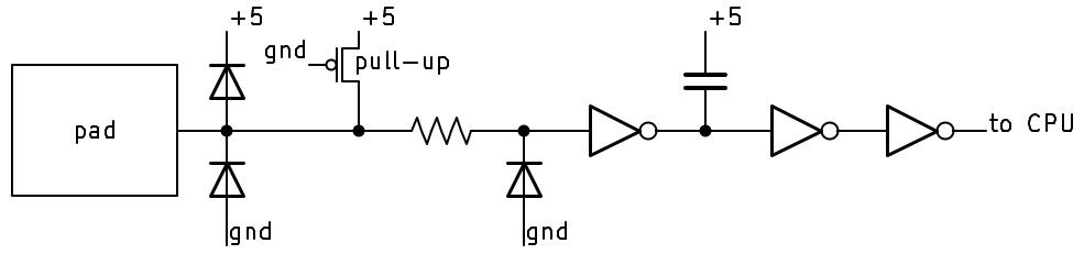
BS16# pad circuit. The BS16# signal indicates to the 386 if the external bus is 16 bits or 32 bits.The image below shows how this circuit appears on the die. For this photo, I dissolved the metal layers with acids, stripping the die down to the silicon to make the transistors visible. The diodes and pull-up resistor are implemented with transistors.3 Large grids of transistors form the pad-side diodes, while the third diode is above. The current-limiting protection resistor is implemented with polysilicon, which provides higher resistance than metal wiring. The capacitor is implemented with a plate of polysilicon over silicon, separated by a thin oxide layer. As you can see, the protection circuitry occupies much more area than the inverters that process the signal.
Latchup
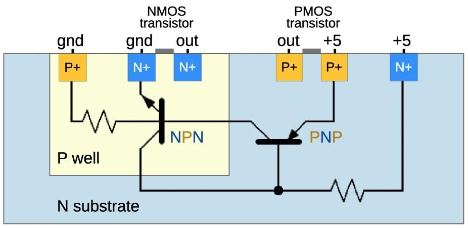
The transistors in the 386 are created by doping silicon with impurities to change its properties, creating regions of "N-type" and "P-type" silicon. The 386 chip, like most processors, is built from CMOS technology, so it uses two types of transistors: NMOS and PMOS. The 386 starts from a wafer of N-type silicon and PMOS transistors are formed by doping tiny regions to form P-type silicon embedded in the underlying N-type silicon. NMOS transistors are the opposite, with N-type silicon embedded in P-type silicon. To hold the NMOS transistors, "wells" of P-type silicon are formed, as shown in the cross-section diagram below. Thus, the 386 chip contains complex patterns of P-type and N-type silicon that form its 285,000 transistors.
But something dangerous lurks below the surface, the fire-breathing dragon of latchup waiting to burn up the chip. The problem is that these regions of N-type and P-type silicon form unwanted, "parasitic" transistors underneath the desired transistors. In normal circumstances, these parasitic NPN and PNP transistors are inactive and can be ignored. But if a current flows beneath the surface, through the silicon substrate, it can turn on a parasitic transistor and awaken the dreaded latchup.4 The parasitic transistors form a feedback loop, so if one transistor starts to turn on, it turns on the other transistor, and so forth, until both transistors are fully on, a state called latchup.5 Moreover, the feedback loop will maintain latchup until the chip's power is removed.6 During latchup, the chip's power and ground are shorted through the parasitic transistors, causing high current flow that can destroy the chip by overheating it or even melting bond wires.
Latchup can be triggered in many ways, from power supply overvoltage to radiation, but a chip's I/O pins are the primary risk because signals from the outside world are unpredictable. For instance, suppose a floppy drive is connected to the 386 and the drive sends a signal with a voltage higher than the 386's 5-volt supply. (This could happen due to a voltage surge in the drive, reflection in a signal line, or even connecting a cable.) Current will flow through the 386's protection diodes, the diodes that were described in the previous section.7 If this current flows through the chip's silicon substrate, it can trigger latchup and destroy the processor.
Because of this danger, the 386's I/O pads are designed to prevent latchup. One solution is to block the unwanted currents through the substrate, essentially putting fences around the transistors to keep malicious currents from escaping into the substrate. In the 386, this fence consists of "guard rings" around the I/O transistors and diodes. These rings prevent latchup by blocking unwanted current flow and safely redirecting it to power or ground.
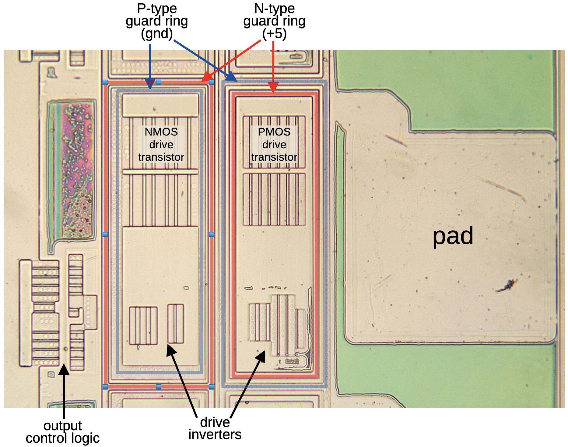
The diagram above shows the double guard rings for a typical I/O pad.8 Separate guard rings protect the NMOS transistors and the PMOS transistors. The NMOS transistors have an inner guard ring of P-type silicon connected to ground (blue) and an outer guard ring of N-type silicon connected to +5 (red). The rings are reversed for the PMOS transistors. The guard rings take up significant space on the die, but this space isn't wasted since the rings protect the chip from latchup.
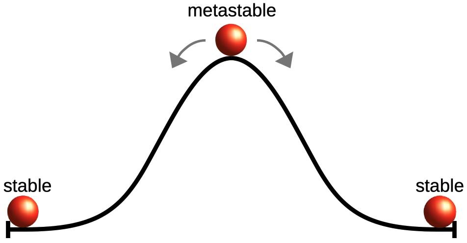
Metastability
The final dragon is metastability: it (probably) won't destroy the chip, but it can cause serious malfunctions.9 Metastability is a peculiar problem where a digital signal can take an unbounded amount of time to settle into a zero or a one. In other words, the circuit temporarily refuses to act digitally and shows its underlying analog nature.10 Metastability was controversial in the 1960s and the 1970s, with many electrical engineers not believing it existed or considering it irrelevant. Nowadays, metastability is well understood, with special circuits to prevent it, but metastability can never be completely eliminated.
In a processor, everything is synchronized to its clock. While a modern processor has a clock speed of several gigahertz, the 386's clock ran at 12 to 33 megahertz. Inside the processor, signals are carefully organized to change according to the clock—that's why your computer runs faster with a higher clock speed. The problem is that external signals may be independent of the CPU's clock. For instance, a disk drive could send an interrupt to the computer when data is ready, which depends on the timing of the spinning disk. If this interrupt arrives at just the wrong time, it can trigger metastability.
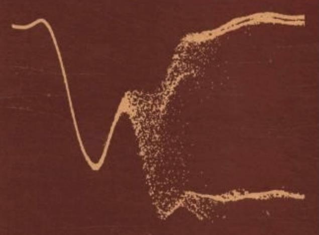
In more detail, processors use flip-flops to hold signals under the control of the clock. An "edge-triggered" flip-flop grabs its input at the moment the clock goes high (the "rising edge") and holds this value until the next clock cycle. Everything is fine if the value is stable when the clock changes: if the input signal switches from low to high before the clock edge, the flip-flop will hold this high value. And if the input signal switches from low to high after the clock edge, the flip-flop will hold the low value, since the input was low at the clock edge. But what happens if the input changes from low to high at the exact time that the clock switches? Usually, the flip-flop will pick either low or high. But very rarely, maybe a few times out of a billion, the flip-flop will hesitate in between, neither low nor high. The flip-flop may take a few nanoseconds before it "decides" on a low or high value, and the value will be intermediate until then.
The photo above illustrates a metastable signal, spending an unpredictable time between zero and one before settling on a value. The situation is similar to a ball balanced on top of a hill, a point of unstable equilibrium.11 The smallest perturbation will knock the ball down one of the two stable positions at the bottom of the hill, but you don't know which way it will go or how long it will take.
A metaphorical view of metastability as a ball on a hill, able to roll down either side.
Metastability is serious because if a digital signal has a value that is neither 0 nor 1 then downstream circuitry may get confused. For instance, if part of the processor thinks that it received an interrupt and other parts of the processor think that no interrupt happened, chaos will reign as the processor takes contradictory actions. Moreover, waiting a few nanoseconds isn't a cure because the duration of metastability can be arbitrarily long. Waiting helps, since the chance of metastability decreases exponentially with time, but there is no guarantee.12
The obvious solution is to never change an input exactly when the clock changes. The processor is designed so that internal signals are stable when the clock changes, avoiding metastability. Specifically, the designer of a flip-flop specifies the setup time—how long the signal must be stable before the clock edge—and the hold time—how long the signal must be stable after the clock edge. As long as the input satisfies these conditions, typically a few picoseconds long, the flip-flop will function without metastability.
Unfortunately, the setup and hold times can't be guaranteed when the processor receives an external signal that isn't synchronized to its clock, known as an asynchronous signal. For instance, a processor receives interrupt signals when an I/O device has data, but the timing is unpredictable because it depends on mechanical factors such as a keypress or a spinning floppy disk. Most of the time, everything will work fine, but what about the one-in-a-billion case where the timing of the signal is unlucky? (Since modern processors run at multi-gigahertz, one-in-a-billion events are not rare; they can happen multiple times per second.)
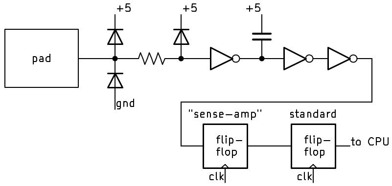
One solution is a circuit called a synchronizer that takes an asynchronous signal and synchronizes it to the clock. A synchronizer can be implemented with two flip-flops in series: even if the first flip-flop has a metastable output, chances are that it will resolve to 0 or 1 before the second flip-flop stores the value. Each flip-flop provides an exponential reduction in the chance of metastability, so using two flip-flops drastically reduces the risk. In other words, the circuit will still fail occasionally, but if the mean time between failures (MTBF) is long enough (say, decades instead of seconds), then the risk is acceptable.
The schematic for the BUSY# pin, showing the flip-flops that synchronize the input signal.
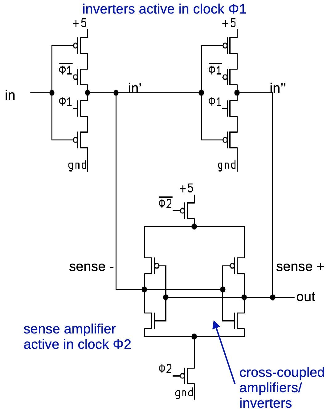
The schematic above shows how the 386 uses two flip-flops to minimize metastability. The first flip-flop is a special flip-flop that is based on a sense amplifier. It is much more complicated than a regular flip-flop, but it responds faster, reducing the chance of metastability. It is built from two of the sense-amplifier latches below, which I haven't seen described anywhere. In a DRAM memory chip, a sense amplifier takes a weak signal from a memory cell and rapidly amplifies it into a solid 0 or 1. In this flip-flop, the sense amplifier takes a potentially ambiguous signal and rapidly amplifies it into a 0 or 1. By amplifying the signal quickly, the flip-flop reduces metastability. (See the footnote for details.14 )
The sense amplifier latch circuit.
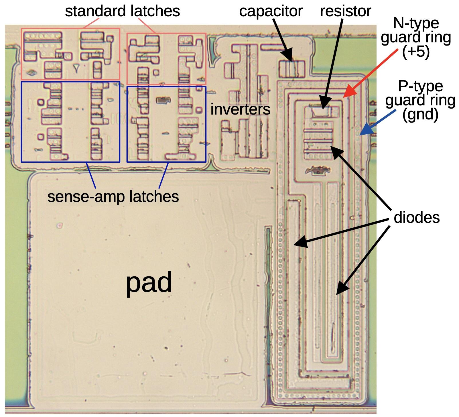
The die photo below shows how this circuitry looks on the die. Each flip-flop is built from two latches; note that the sense-amp latches are larger than the standard latches. As before, the pad has protection diodes inside guard rings. For some reason, however, these diodes have a different structure from the transistor-based diodes described earlier. The 386 has five inputs that use this circuitry to protect against metastability.13 These inputs are all located together at the bottom of the die—it probably makes the layout more compact when neighboring pad circuits are all the same size.
In summary, the 386's I/O circuits are interesting because they are completely different from the chip's regular logic circuitry. In these circuits, the border between digital and analog breaks down; these circuits handle binary signals, but analog issues dominate the design. Moreover, hidden parasitic transistors play key roles; what you don't see can be more important than what you see. These circuits defend against three dangerous "dragons": static electricity, latchup, and metastability. Intel succeeded in warding off these dragons and the 386 was a success.
For more on the 386 and other chips, follow me on Mastodon (@[email protected]), Bluesky (@righto.com), or RSS. (I've given up on Twitter.) If you want to read more about 386 input circuits, I wrote about the clock pin here
Notes and references
-
Anti-static precautions are specified in Intel's processor installation instructions. Also see Intel's Electrostatic Discharge and Electrical Overstress Guide. I couldn't find ESD ratings for the 386, but a modern Intel chip is tested to withstand 500 volts or 2000 volts, depending on the test procedure. ↩
-
The BS16# pin is slightly unusual because it has an internal pull-up resistor. If you look at the datasheet (9.2.3 and Table 9-3 footnotes), a few input pins (ERROR#, BUSY#, and BS16#) have internal pull-up resistors of 20 kΩ, while the PEREQ input pin has an internal pull-down resistor of 20 kΩ. ↩
-
The protection diode is probably a grounded-gate NMOS (ggNMOS), an NMOS transistor with the gate, source, and body (but not the drain) tied to ground. This forms a parasitic NPN transistor under the MOSFET that dissipates the ESD. (I think that the PMOS protection is the same, except the gate is pulled high, not grounded.) For output pins, the output driver MOSFETs have parasitic transistors that make the output driver "self-protected". One consequence is that the input pads and the output pads look similar (both have large MOS transistors), unlike other chips where the presence of large transistors indicates an output. (Even so, 386 outputs and inputs can be distinguished because outputs have large inverters inside the guard rings to drive the MOSFETs, while inputs do not.) Also see Practical ESD Protection Design. ↩
-
The 386 uses P-wells in an N-doped substrate. The substrate is heavily doped with antimony, with a lightly doped N epitaxial layer on top. This doping helped provide immunity to latchup. (See "High performance technology, circuits and packaging for the 80386", ICCD 1986.) For the most part, modern chips use the opposite: N-wells with a P-doped substrate. Why the substrate change?
In the earlier days of CMOS, P-well was standard due to the available doping technology, see N-well and P-well performance comparison. During the 1980s, there was controversy over which was better: P-well or N-well: "It is commonly agreed that P-well technology has a proven reliability record, reduced alpha-particle sensitivity, closer matched p- and n- channel devices, and high gain NPN structures. N-well proponents acknowledge better compatibility and performance with NMOS processing and designs, good substrate quality, availability, and cost, lower junction capacitance, and reduced body effects." (See Design of a CMOS Standard Cell Library.)
As wafer sizes increased in the 1990s, technology shifted to P-doped substrates because it is difficult to make large N-doped wafers due to the characteristics of the dopants (link). Some chips optimize transistor characteristics by using both types of wells, called a twin-well process. For instance, the Pentium used P-doped wafers and implanted both N and P wells. (See Intel's 0.25 micron, 2.0 volts logic process technology.) ↩
-
You can also view the parasitic transistors as forming an SCR (Silicon Controlled Rectifier), a four-layer semiconductor device. SCRs were popular in the 1970s because they could handle higher currents and voltages than transistors. But as high-power transistors were developed, SCRs fell out of favor. In particular, once an SCR is turned on, it stays on until power is removed or reversed; this makes SCRs harder to use than transistors. (This is the same characteristic that makes latchup so dangerous.) ↩
-
Satellites and nuclear missiles have a high risk of latchup due to radiation. Since radiation-induced latchup cannot always be prevented, one technique for dealing with latchup is to detect the excessive current from latchup and then power-cycle the chip. For instance, you can buy a radiation-hardened current limiter chip that will detect excessive current due to latchup and temporarily remove power; this chip sells for the remarkable price of 1780ドル.
For more on latchup, see the Texas Instruments Latch-Up white paper, as well as Latch-Up, ESD, and Other Phenomena. ↩
-
The 80386 Hardware Reference Manual discusses how a computer designer can prevent latchup in the 386. The designer is assured that Intel's "CHMOS III" process prevents latchup under normal operating conditions. However, exceeding the voltage limits on I/O pins can cause current surges and latchup. Intel provides three guidelines: observe the maximum ratings for input voltages, never apply power to a 386 pin before the chip is powered up, and terminate I/O signals properly to avoid overshoot and undershoot. ↩
-
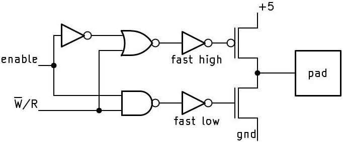
The circuit for the WR# pin is similar to many other output pins. The basic idea is that a large PMOS transistor pulls the output high, while a large NMOS transistor pulls the output low. If the
enableinput is low, both transistors are turned off and the output floats. (This allows other devices to take over the bus in the HOLD state.)Schematic for the WR# pin driver.
Schematic for the WR# pin driver.The inverters that control the drive transistors have an unusual layout. These inverters are inside the guard rings, meaning that the inverters are split apart, with the NMOS transistors in one ring and PMOS transistors in the other. The extra wiring adds capacitance to the output which probably makes the inverters slightly slower.
These inverters have a special design: one inverter is faster to go high than to go low, while the other inverter is the opposite. The motivation is that if both drive transistors are on at the same time, a large current will flow through the transistors from power to ground, producing an unwanted current spike (and potentially latchup). To avoid this, the inverters are designed to turn one drive transistor off faster than turning the other one on. Specifically, the high-side inverter has an extra transistor to quickly pull its output high, while the low-side inverter has an extra transistor to pull the output low. Moreover, the inverter's extra transistor is connected directly to the drive transistors, while the inverter's main output connects through a longer polysilicon path with more resistance, providing an RC delay. I found this layout very puzzling until I realized that the designers were carefully controlling the turn-on and turn-off speeds of these inverters. ↩
-
In Metastability and Synchronizers: A Tutorial, there's a story of a spacecraft power supply being destroyed by metastability. Supposedly, metastability caused the logic to turn on too many units, overloading and destroying the power supply. I suspect that this is a fictional cautionary tale, rather than an actual incident.
For more on metastability, see this presentation and this writeup by Tom Chaney, one of the early investigators of metastability. ↩
-
One of Vonada's Engineering Maxims is "Digital circuits are made from analog parts." Another maxim is "Synchronizing circuits may take forever to make a decision." These maxims and a dozen others are from Don Vonada in DEC's 1978 book Computer Engineering. ↩
-
Curiously, the definition of metastability in electronics doesn't match the definition in physics and chemistry. In electronics, a metastable state is an unstable equilibrium. In physics and chemistry, however, a metastable state is a stable state, just not the most stable ground state, so a moderate perturbation will knock it from the metastable state to the ground state. (In the hill analogy, it's as if the ball is caught in a small basin partway down the hill.) ↩
-
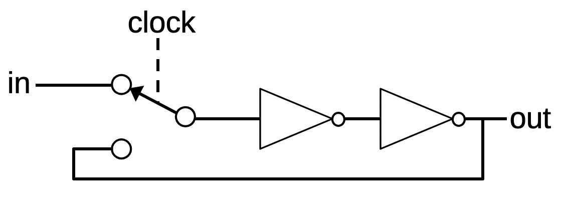
In case you're wondering what's going on with metastability at the circuit level, I'll give a brief explanation. A typical flip-flop is based on a latch circuit like the one below, which consists of two inverters and an electronic switch controlled by the clock. When the clock goes high, the inverters are configured into a loop, latching the prior input value. If the input was high, the output from the first inverter is low and the output from the second inverter is high. The loop feeds this output back into the first inverter, so the circuit is stable. Likewise, the circuit can be stable with a low input.
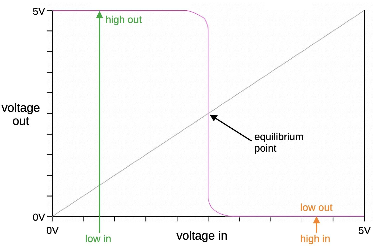
A latch circuit.But what happens if the clock flips the switch as the input is changing, so the input to the first inverter is somewhere between zero and one? We need to consider that an inverter is really an analog device, not a binary device. You can describe it by a "voltage transfer curve" (purple line) that specifies the output voltage for a particular input voltage. For example, if you put in a low input, you get a high output, and vice versa. But there is an equilibrium point where the output voltage is the same as the input voltage. This is where metastability happens.
The voltage transfer curve for a hypothetical inverter.
The voltage transfer curve for a hypothetical inverter.Suppose the input voltage to the inverter is the equilibrium voltage. It's not going to be precisely the equilibrium voltage (because of noise if nothing else), so suppose, for example, that it is 1μV above equilibrium. Note that the transfer curve is very steep around equilibrium, say a slope of 100, so it will greatly amplify the signal away from equilibrium. Thus, if the input is 1μV above equilibrium, the output will be 100μV below equilibrium. Then the next inverter will amplify again, sending a signal 10mV above equilibrium back to the first inverter. The distance will be amplified again, now 1000mV below equilibrium. At this point, you're on the flat part of the curve, so the second inverter will output +5V and the first inverter will output 0V, and the circuit is now stable.
The point of this is that the equilibrium voltage is an unstable equilibrium, so the circuit will eventually settle into the +5V or 0V states. But it may take an arbitrary number of loops through the inverters, depending on how close the starting point was to equilibrium. (The signal is continuous, so referring to "loops" is a simplification.) Also note that the distance from equilibrium is amplified exponentially with time. This is why the chance of metastability decreases exponentially with time. ↩
-
Looking at the die shows that the pins with metastability protection are
INTR,NMI,PEREQ,ERROR#, andBUSY#. The 80386 Hardware Reference Manual lists these same five pins as asynchronous—I like it when I spot something unusual on the die and then discover that it matches an obscure statement in the documentation. The interrupt pinsINTRandNMIare asynchronous because they come from external sources that may not be using the 386's clock. But what aboutPEREQ,ERROR#, andBUSY#? These pins are part of the interface with an external math coprocessor (the 287 or 387 chip). In most cases, the coprocessor uses the 386's clock. However, the 387 supported a little-used asynchronous mode where the processor and the coprocessor could run at different speeds. ↩ -
The 386's metastability flip-flop is constructed with an unusual circuit. It has two latch stages (which is normal), but instead of using two inverters in a loop, it uses a sense-amplifier circuit. The idea of the sense amplifier is that it takes a differential input. When the clock enables the sense amplifier, it drives the higher input high and the lower input low (the inputs are also the outputs). (Sense amplifiers are used in dynamic RAM chips to amplify the tiny signals from a RAM cell to form a 0 or 1. At the same time, the amplifier refreshes the DRAM cell by generating full voltages.) Note that the sense amplifier's inputs also act as outputs; inputs during clock phase 1 and outputs during phase 2.
The schematic shows one of the latch stages; the complete flip-flop has a second stage, identical except that the clock phases are switched. This latch is much more complex than the typical 386 latch; 14 transistors versus 6 or 8. The sense amplifier is similar to two inverters in a loop, except they share a limited power current and a limited ground current. As one inverter starts to go high, it "steals" the supply current from the other. Meanwhile, the other inverter "steals" the ground current. Thus, a small difference in inputs is amplified, just as in a differential amplifier. Thus, by combining the amplification of a differential amplifier with the amplification of the inverter loop, this circuit reaches its final state faster than a regular inverter loop.
In more detail, during the first clock phase, the two inverters at the top generate the inverted and non-inverted signals. (In a metastable situation, these will be close to the midpoint, not binary.) During the second clock phase, the sense amplifier is activated. You can think of it as a differential amplifier with cross-coupling. If one input is slightly higher than the other, the amplifier pulls that input higher and the input lower, amplifying the difference. (The point is to quickly make the difference large enough to resolve the metastability.)
I couldn't find any latches like this in the literature. Comparative Analysis and Study of Metastability on High-Performance Flip-Flops describes eleven high-performance flip-flops. It includes two flip-flops that are based on sense amplifiers, but their circuits are very different from the 386 circuit. Perhaps the 386 circuit is an Intel design that was never publicized. In any case, let me know if this circuit has an official name. ↩
A CT scanner reveals surprises inside the 386 processor's ceramic package
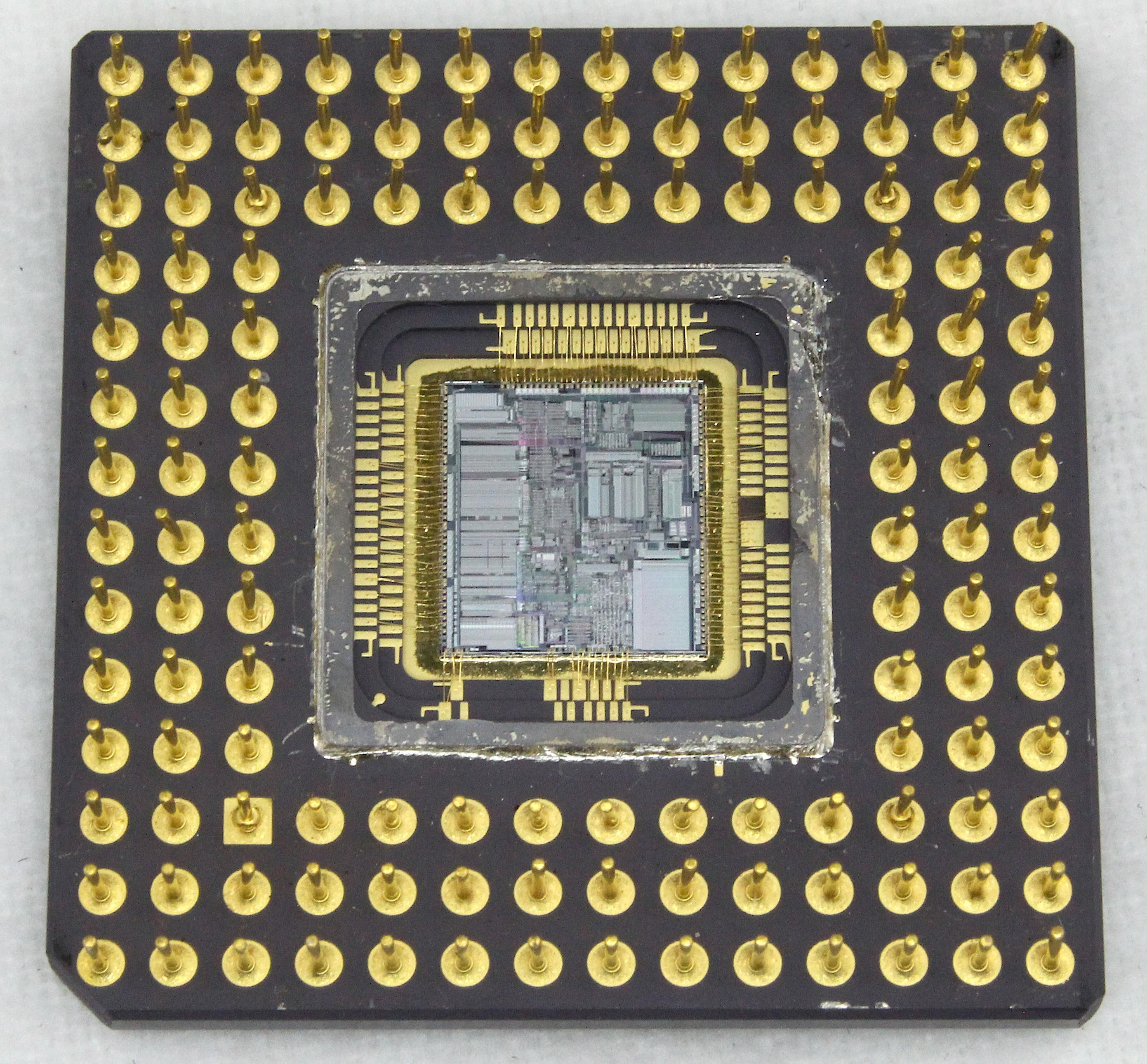
Intel released the 386 processor in 1985, the first 32-bit chip in the x86 line. This chip was packaged in a ceramic square with 132 gold-plated pins protruding from the underside, fitting into a socket on the motherboard. While this package may seem boring, a lot more is going on inside it than you might expect. Lumafield performed a 3-D CT scan of the chip for me, revealing six layers of complex wiring hidden inside the ceramic package. Moreover, the chip has nearly invisible metal wires connected to the sides of the package, the spikes below. The scan also revealed that the 386 has two separate power and ground networks: one for I/O and one for the CPU's logic.
The package, below, provides no hint of the complex wiring embedded inside the ceramic. The silicon die is normally not visible, but I removed the square metal lid that covers it.1 As a result, you can also see the two tiers of gold contacts that surround the silicon die.
The 386 package with the lid over the die removed.
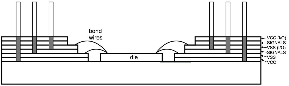
Intel selected the 132-pin ceramic package to meet the requirements of a high pin count, good thermal characteristics, and low-noise power to the die.2 : However, standard packages didn't provide sufficient power, so Intel designed a custom package with "single-row double shelf bonding to two signal layers and four power and ground planes." In other words, the die's bond wires are connected to the two shelves (or tiers) of pads surrounding the die. Internally, the package is like a 6-layer printed-circuit board made from ceramic.
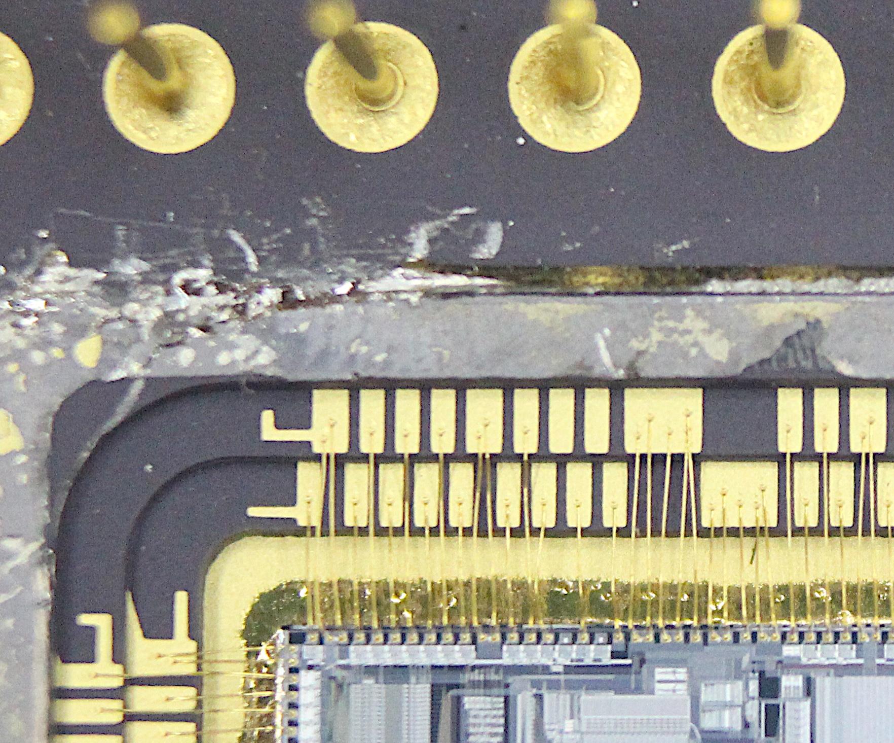
The photo below shows the two tiers of pads with tiny gold bond wires attached: I measured the bond wires at 35 μm in diameter, thinner than a typical human hair. Some pads have up to five wires attached to support more current for the power and ground pads. You can consider the package to be a hierarchical interface from the tiny circuits on the die to the much larger features of the computer's motherboard. Specifically, the die has a feature size of 1 μm, while the metal wiring on top of the die has 6 μm spacing. The chip's wiring connects to the chip's bond pads, which have 0.01" spacing (.25 mm). The bond wires connect to the package's pads, which have 0.02" spacing (.5 mm); double the spacing because there are two tiers. The package connects these pads to the pin grid with 0.1" spacing (2.54 mm). Thus, the scale expands by about a factor of 2500 from the die's microscopic circuitry to the chip's pins. `
The ceramic package is manufactured through a complicated process.4 The process starts with flexible ceramic "green sheets", consisting of ceramic powder mixed with a binding agent. After holes for vias are created in the sheet, tungsten paste is silk-screened onto the sheet to form the wiring. The sheets are stacked, laminated under pressure, and then sintered at high temperature (1500oC to 1600oC) to create the rigid ceramic. The pins are brazed onto the bottom of the chip. Next, the pins and the inner contacts for the die are electroplated with gold.3 The die is mounted, gold bond wires are attached, and a metal cap is soldered over the die to encapsulate it. Finally, the packaged chip is tested, the package is labeled, and the chip is ready to be sold.
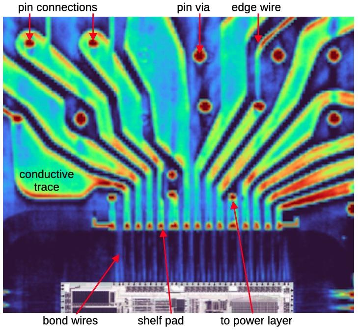
The diagram below shows a close-up of a signal layer inside the package. The pins are connected to the package's shelf pads through metal traces, spectacularly colored in the CT scan. (These traces are surprisingly wide and free-form; I expected narrower traces to reduce capacitance.) Bond wires connect the shelf pads to the bond pads on the silicon die. (The die image is added to the diagram; it is not part of the CT scan.) The large red circles are vias from the pins. Some vias connect to this signal layer, while other vias pass through to other layers. The smaller red circles are connections to a power layer; because the shelf pads are only on the two signal layers, the six power planes have connections to the signal layers for bonding. Since bond wires are only connected on the signal layers, the power layers need connections to pads on the signal layers.
A close-up of a signal layer. The die image is pasted in.
The diagram below shows the corresponding portion of a power layer. A power layer looks completely different from a signal layer; it is a single conductive plane with holes. The grid of smaller holes allows the ceramic above and below this layer to bond, forming a solid piece of ceramic. The larger holes surround pin vias (red dots), allowing pin connections to pass through to a different layer. The red dots that contact the sheet are where power pins connect to this layer. Because the only connections to the die are from the signal layers, the power layers have connections to the signal layers; these are the smaller dots near the bond wires, either power vias passing through or vias connected to this layer.
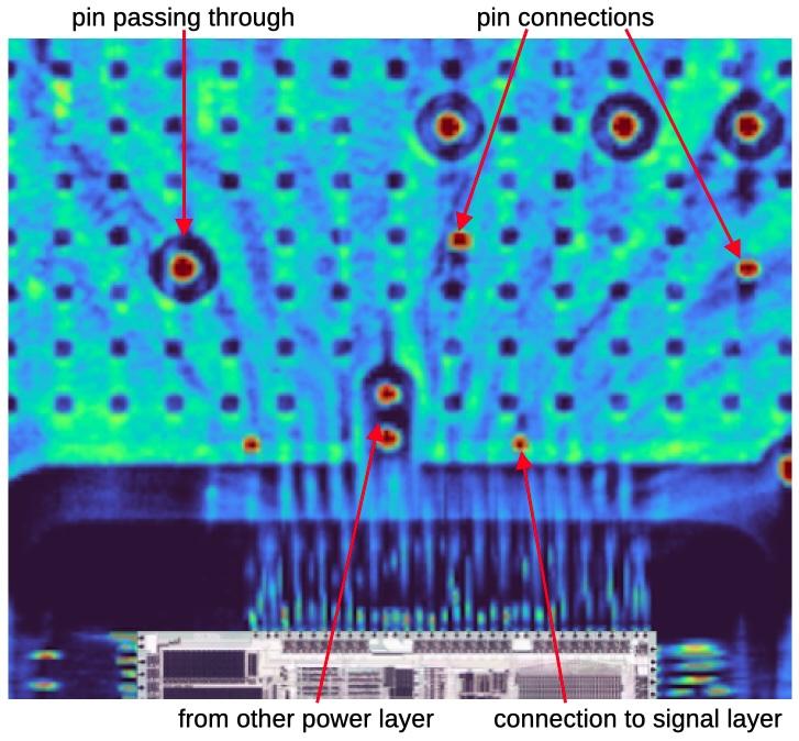
With the JavaScript tool below, you can look at the package, layer by layer. Click on a radio button to select a layer. By observing the path of a pin through the layers, you can see where it ends up. For instance, the upper left pin passes through multiple layers until the upper signals layer connects it to the die. The pin to its right passes through all the layers until it reaches the logic Vcc plane on top. (Vcc is the 5-volt supply that powers the chip, called Vcc for historical reasons.)
If you select the logic Vcc plane above, you'll see a bright blotchy square in the center. This is not the die itself, I think, but the adhesive that attaches the die to the package, epoxy filled with silver to provide thermal and electrical conductivity. Since silver blocks X-rays, it is highly visible in the image.
Side contacts for electroplating
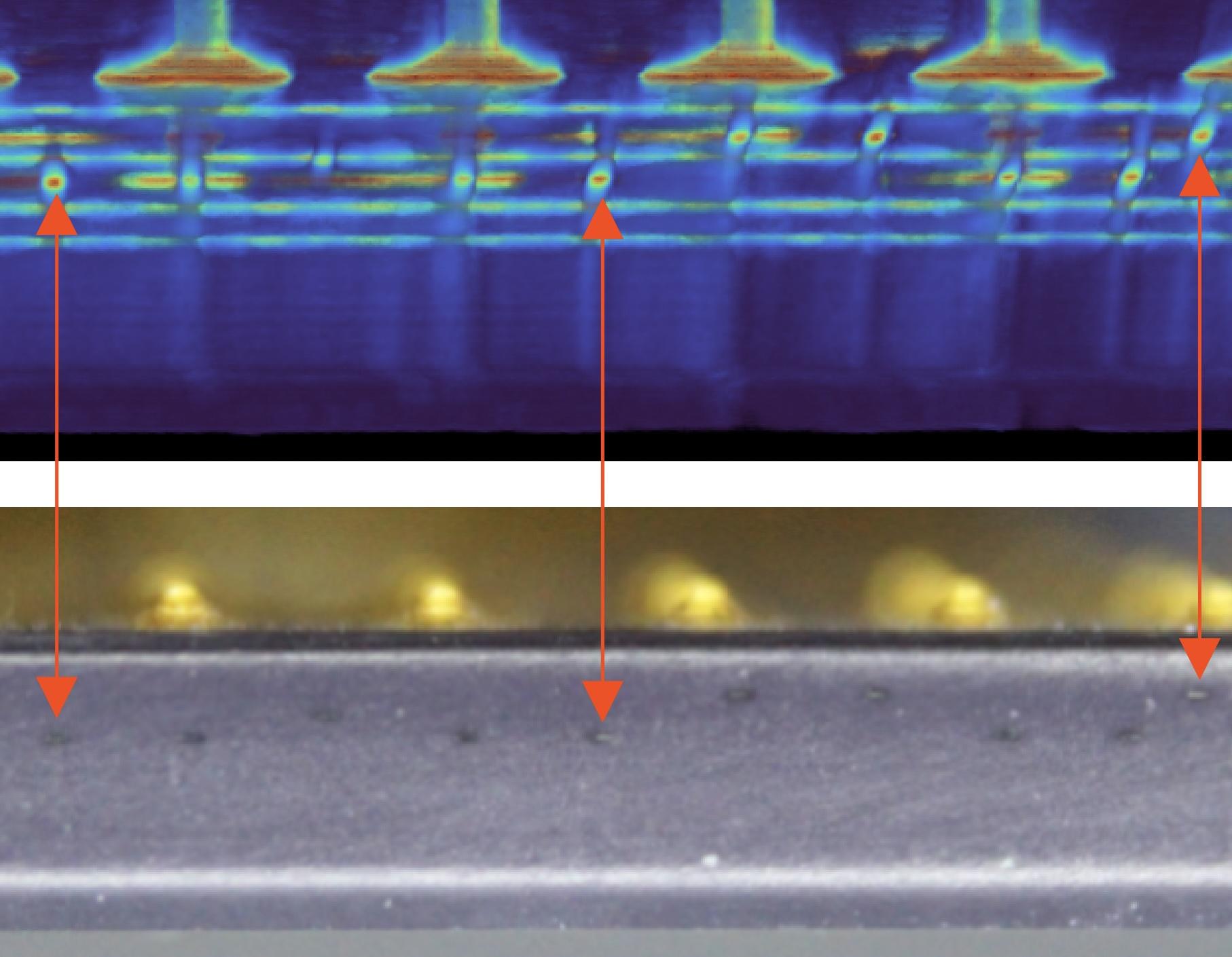
What surprised me most about the scans was seeing wires that stick out to the sides of the package. These wires are used during manufacturing when the pins are electroplated with gold.5 In order to electroplate the pins, each pin must be connected to a negative voltage so it can function as a cathode. This is accomplished by giving each pin a separate wire that goes to the edge of the package.
This diagram below compares the CT scan (above) to a visual side view of the package (below). The wires are almost invisible, but can be seen as darker spots. The arrows show how three of these spots match with the CT scan; you can match up the other spots.6
Two power networks
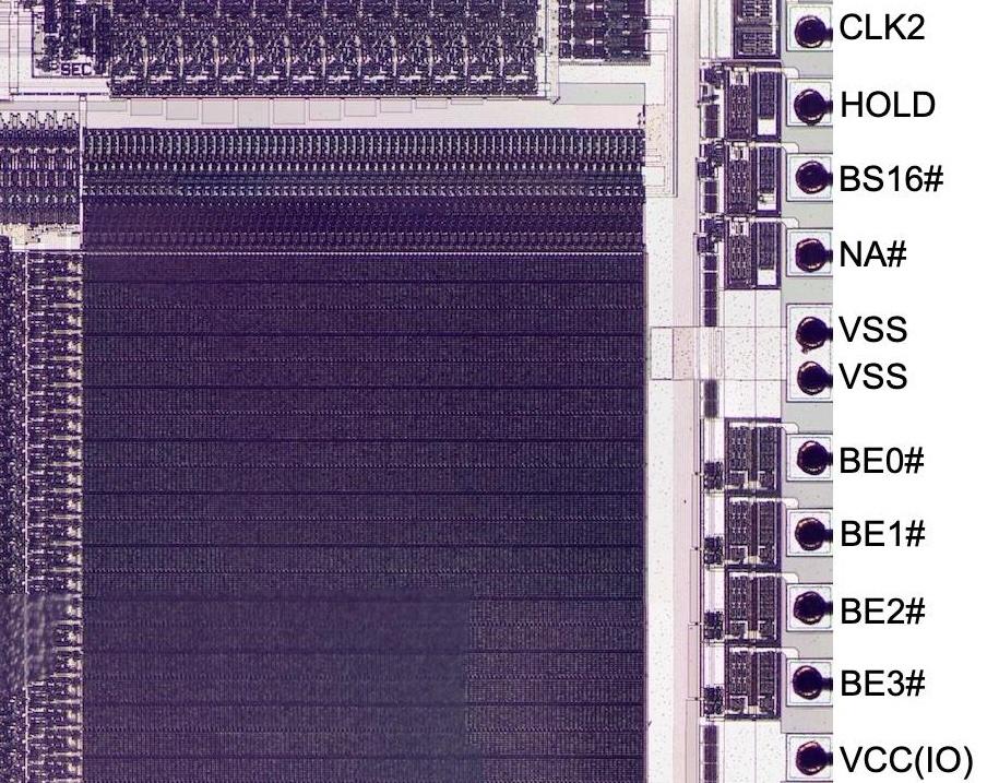
According to the datasheet, the 386 has 20 pins connected to +5V power (Vcc) and 21 pins connected to ground (Vss). Studying the die, I noticed that the I/O circuitry in the 386 has separate power and ground connections from the logic circuitry. The motivation is that the output pins require high-current driver circuits. When a pin switches from 0 to 1 or vice versa, this can cause a spike on the power and ground wiring. If this spike is too large, it can interfere with the processor's logic, causing malfunctions. The solution is to use separate power wiring inside the chip for the I/O circuitry and for the logic circuitry, connected to separate pins. On the motherboard, these pins are all connected to the same power and ground, but decoupling capacitors absorb the I/O spikes before they can flow into the chip's logic.
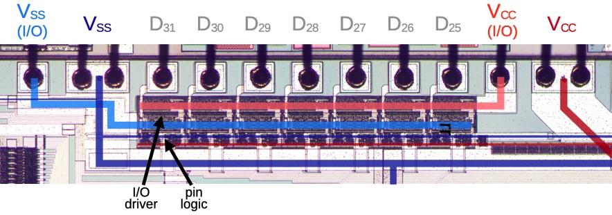
The diagram below shows how the two power and ground networks look on the die, with separate pads and wiring. The square bond pads are at the top, with dark bond wires attached. The white lines are the two layers of metal wiring, and the darker regions are circuitry. Each I/O pin has a driver circuit below it, consisting of relatively large transistors to pull the pin high or low. This circuitry is powered by the horizontal lines for I/O Vcc (light red) and I/O ground (Vss, light blue). Underneath each I/O driver is a small logic circuit, powered by thinner Vcc (dark red) and Vss (dark blue). Thicker Vss and Vcc wiring goes to the logic in the rest of the chip. Thus, if the I/O circuitry causes power fluctuations, the logic circuit remains undisturbed, protected by its separate power wiring.
A close-up of the top of the die, showing the power wiring and the circuitry for seven data pins.
The datasheet doesn't mention the separate I/O and logic power networks, but by using the CT scans, I determined which pins power I/O, and which pins power logic. In the diagram below, the light red and blue pins are power and ground for I/O, while the dark red and blue pins are power and ground for logic. The pins are scattered across the package, allowing power to be supplied to all four sides of the die.
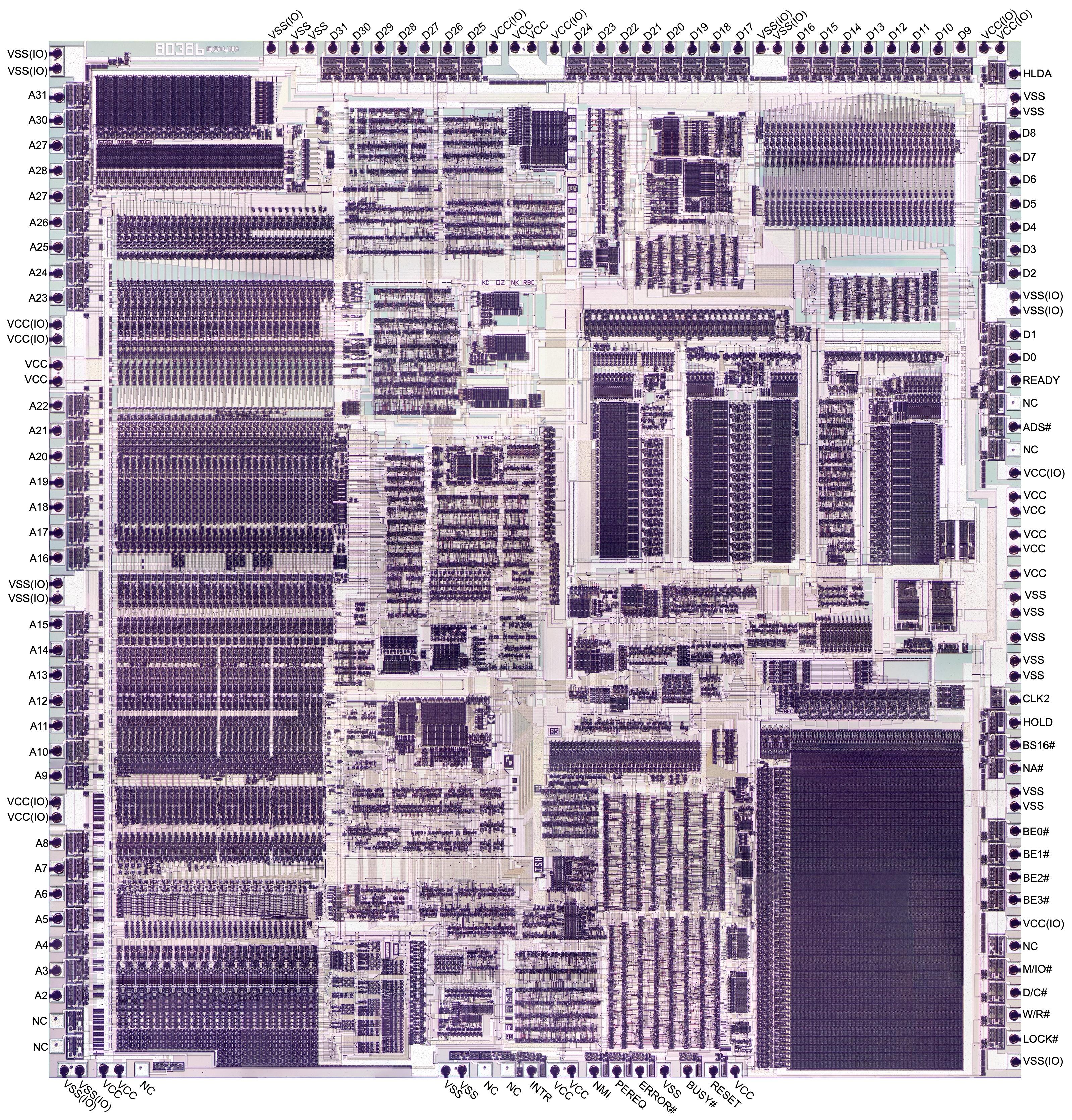
The pinout from the Intel386DX Microprocessor Datasheet. This is the view from the pin side.
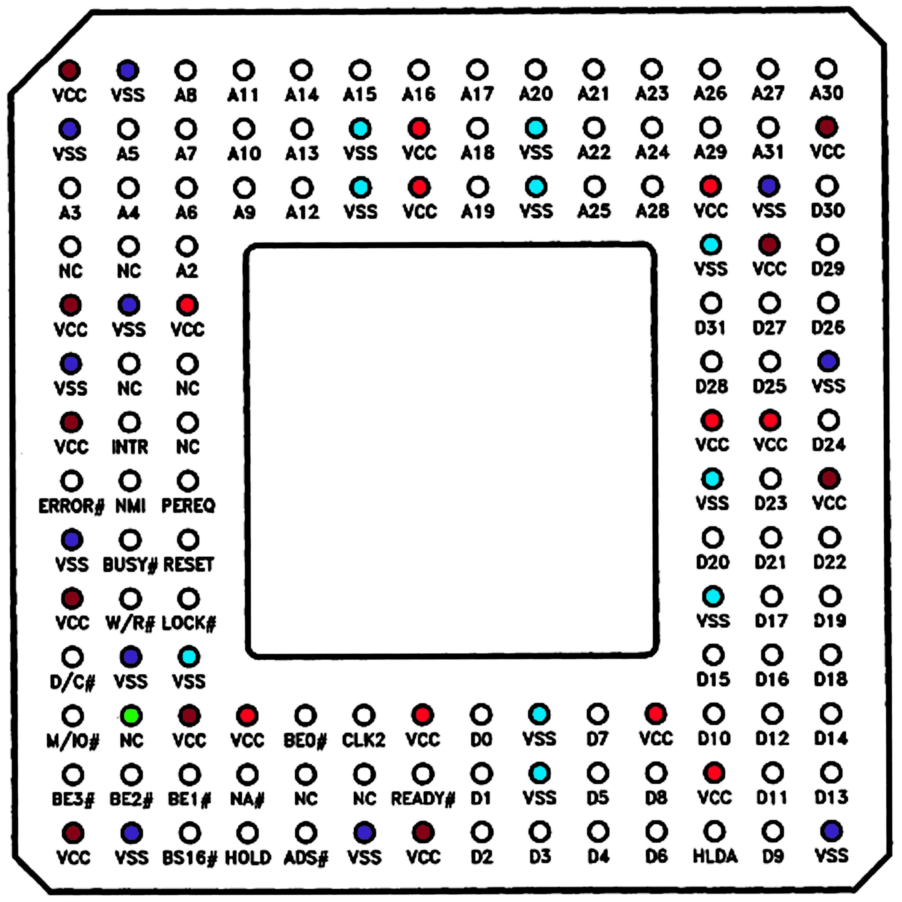
"No Connect" pins
As the diagram above shows, the 386 has eight pins labeled "NC" (No Connect)—when the chip is installed in a computer, the motherboard must leave these pins unconnected. You might think that the 132-pin package simply has eight extra, unneeded pins, but it's more complicated than that. The photo below shows five bond pads at the bottom of the 386 die. Three of these pads have bond wires attached, but two have no bond wires: these correspond to No Connect pins. Note the black marks in the middle of the pads: the marks are from test probes that were applied to the die during testing.7 The No Connect pads presumably have a function during this testing process, providing access to an important internal signal.
A close-up of the die showing three bond pads with bond wires and two bond pads without bond wires.
Seven of the eight No Connect pads are almost connected: the package has a spot for a bond wire in the die cavity and the package has internal wiring to a No Connect pin. The only thing missing is the bond wire between the pad and the die cavity. Thus, by adding bond wires, Intel could easily create special chips with these pins connected, perhaps for debugging the test process itself.
The surprising thing is that one of the No Connect pads does have the bond wire in place, completing the connection to the external pin. (I marked this pin in green in the pinout diagram earlier.) From the circuitry on the die, this pin appears to be an output. If someone with a 386 chip hooks this pin to an oscilloscope, maybe they will see something interesting.
Labeling the pads on the die
The earlier 8086 processor, for example, is packaged in a DIP (Dual-Inline Package) with two rows of pins. This makes it straightforward to figure out which pin (and thus which function) is connected to each pad on the die. However, since the 386 has a two-dimensional grid of pins, the mapping to the pads is unclear. You can guess that pins are connected to a nearby pad, but ambiguity remains. Without knowing the function of each pad, I have a harder time reverse-engineering the die.
In fact, my primary motivation for scanning the 386 package was to determine the pin-to-pad mapping and thus the function of each pad.8 Once I had the CT data, I was able to trace out each hidden connection between the pad and the external pin. The image below shows some of the labels; click here for the full, completely labeled image. As far as I know, this information hasn't been available outside Intel until now.
A close-up of the 386 die showing the labels for some of the pins.
Conclusions
Intel's early processors were hampered by inferior packages, but by the time of the 386, Intel had realized the importance of packaging. In Intel's early days, management held the bizarre belief that chips should never have more than 16 pins, even though other companies used 40-pin packages. Thus, Intel's first microprocessor, the 4004 (1971), was crammed into a 16-pin package, limiting its performance. By 1972, larger memory chips forced Intel to move to 18-pin packages, extremely reluctantly.9 The eight-bit 8008 processor (1972) took advantage of this slightly larger package, but performance still suffered because signals were forced to share pins. Finally, Intel moved to the standard 40-pin package for the 8080 processor (1974), contributing to the chip's success. In the 1980s, pin-grid arrays became popular in the industry as chips required more and more pins. Intel used a ceramic pin grid array (PGA) with 68 pins for the 186 and 286 processors (1982), followed by the 132-pin package for the 386 (1985).
The main drawback of the ceramic package was its cost. According to the 386 oral history, the cost of the 386 die decreased over time to the point where the chip's package cost as much as the die. To counteract this, Intel introduced a low-cost plastic package for the 386 that cost just a dollar to manufacture, the Plastic Quad Flat Package (PQFP) (details).
In later Intel processors, the number of connections exponentially increased. A typical modern laptop processor uses a Ball Grid Array with 2049 solder balls; the chip is soldered directly onto the circuit board. Other Intel processors use a Land Grid Array (LGA): the chip has flat contacts called lands, while the socket has the pins. Some Xeon processors have 7529 contacts, a remarkable growth from the 16 pins of the Intel 4004.
From the outside, the 386's package looks like a plain chunk of ceramic. But the CT scan revealed surprising complexity inside, from numerous contacts for electroplating to six layers of wiring. Perhaps even more secrets lurk in the packages of modern processors.
Follow me on Bluesky (@righto.com), Mastodon (@[email protected]), or RSS. (I've given up on Twitter.) Thanks to Jon Bruner and Lumafield for scanning the chip. Lumafield's interactive CT scan of the 386 package is available here if you to want to examine it yourself. Lumafield also scanned a 1960s cordwood flip-flop and the Soviet Globus spacecraft navigation instrument for us. Thanks to John McMaster for taking 2D X-rays.
Notes and references
-
I removed the metal lid with a chisel, as hot air failed to desolder the lid. A few pins were bent in the process, but I straightened them out, more or less. ↩
-
The 386 package is described in "High Performance Technology, Circuits and Packaging for the 80386", Proceedings, ICCD Conference, Oct. 1986. (Also see Design and Test of the 80386 by Pat Gelsinger, former Intel CEO.)
The paper gives the following requirements for the 386 package:
- Large pin count to handle separate 32-bit data and address buses.
- Thermal characteristics resulting in junction temperatures under 110°.
- Power supply to the chip and I/O able to supply 600mA/ns with noise levels less than 0.4V (chip) and less than 0.8V (I/O).
The first and second criteria motivated the selection of a 132-pin ceramic pin grid array (PGA). The custom six-layer package was designed to achieve the third objective. The power network is claimed to have an inductance of 4.5 nH per power pad on the device, compared to 12-14 nH for a standard package, about a factor of 3 better.
The paper states that logic Vcc, logic Vss, I/O Vcc, and I/O Vss each have 10 pins assigned. Curiously, the datasheet states that the 386 has 20 Vcc pins and 21 Vss pins, which doesn't add up. From my investigation, the "extra" pin is assigned to logic Vss, which has 11 pins. ↩
-
I estimate that the 386 package contains roughly 0.16 grams of gold, currently worth about 16ドル. It's hard to find out how much gold is in a processor since online numbers are all over the place. Many people recover the gold from chips, but the amount of gold one can recover depends on the process used. Moreover, people tend to keep accurate numbers to themselves so they can profit. But I made some estimates after searching around a bit. One person reports 9.69g of gold per kilogram of chips, and other sources seem roughly consistent. A ceramic 386 reportedly weighs 16g. This works out to 160 mg of gold per 386. ↩
-
I don't have information on Intel's package manufacturing process specifically. This description is based on other descriptions of ceramic packages, so I don't guarantee that the details are correct for the 386. A Fujitsu patent, Package for enclosing semiconductor elements, describes in detail how ceramic packages for LSI chips are manufactured. IBM's process for ceramic multi-chip modules is described in Multi-Layer Ceramics Manufacturing, but it is probably less similar. ↩
-
An IBM patent, Method for shorting pin grid array pins for plating, describes the prior art of electroplating pins with nickel and/or gold. In particular, it describes using leads to connect all input/output pins to a common bus at the edge of the package, leaving the long leads in the structure. This is exactly what I see in the 386 chip. The patent mentions that a drawback of this approach is that the leads can act as antennas and produce signal cross-talk. Fujitsu patent Package for enclosing semiconductor elements also describes wires that are exposed at side surfaces. This patent covers methods to avoid static electricity damage through these wires. (Picking up a 386 by the sides seems safe, but I guess there is a risk of static damage.)
Note that each input/output pin requires a separate wire to the edge. However, the multiple pins for each power or ground plane are connected inside the package, so they do not require individual edge connections; one or two suffice. ↩
-
To verify that the wires from pins to the edges of the chip exist and are exposed, I used a multimeter and found connectivity between pins and tiny spots on the sides of the chip. ↩
-
To reduce costs, each die is tested while it is still part of the silicon wafer and each faulty die is marked with an ink spot. The wafer is "diced", cutting it apart into individual dies, and only the functional, unmarked dies are packaged, avoiding the cost of packaging a faulty die. Additional testing takes place after packaging, of course. ↩
-
I tried several approaches to determine the mapping between pads and pins before using the CT scan. I tried to beep out the connections between the pins and the pads with a multimeter, but because the pads are so tiny, the process was difficult, error-prone, and caused damage to the package.
I also looked at the pinout of the 386 in a plastic package (datasheet). Since the plastic package has the pins in a single ring around the border, the mapping to the die is straightforward. Unfortunately, the 386 die was slightly redesigned at this time, so some pads were moved around and new pins were added, such as
FLT#. It turns out that the pinout for the plastic chip almost matches the die I examined, but not quite. ↩ -
In his oral history, Federico Faggin, a designer of the 4004, 8008, and Z80 processors, describes Intel's fixation on 16-pin packages. When a memory chip required 18 pins instead of 16, it was "like the sky had dropped from heaven. I never seen so [many] long faces at Intel, over this issue, because it was a religion in Intel; everything had to be 16 pins, in those days. It was a completely silly requirements [sic] to have 16 pins." At the time, other manufacturers were using 40- and 48-pin packages, so there was no technical limitation, just a minor cost saving from the smaller package. ↩