Solving the NYTimes Pips puzzle with a constraint solver
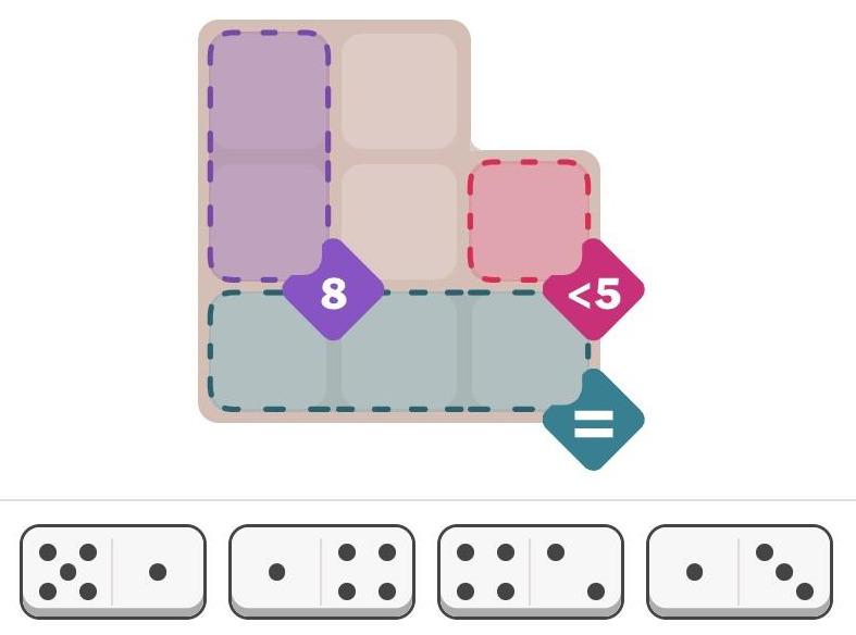
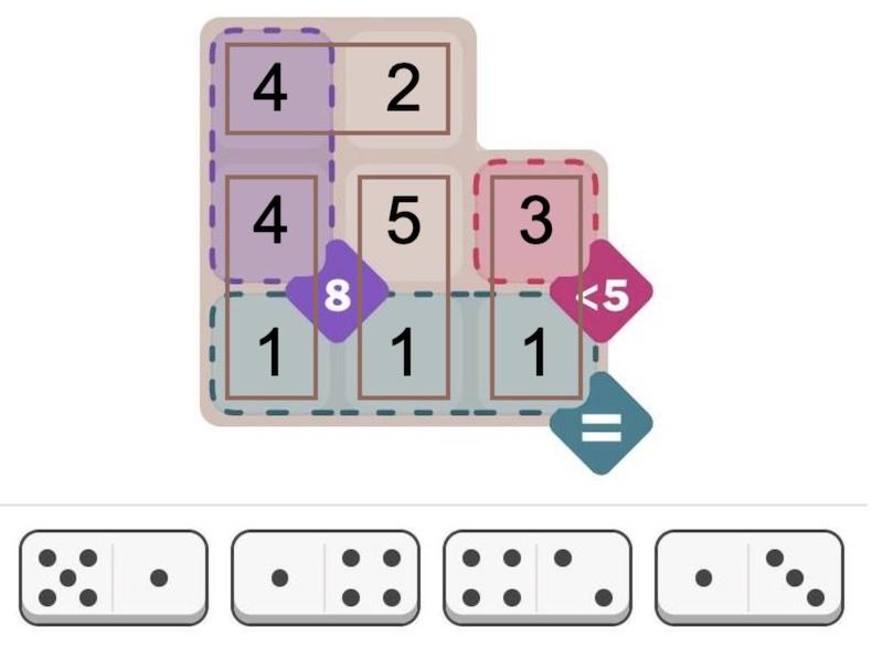
The New York Times recently introduced a new daily puzzle called Pips. You place a set of dominoes on a grid, satisfying various conditions. For instance, in the puzzle below, the pips (dots) in the purple squares must sum to 8, there must be fewer than 5 pips in the red square, and the pips in the three green squares must be equal. (It doesn't take much thought to solve this "easy" puzzle, but the "medium" and "hard" puzzles are more challenging.)
I was wondering about how to solve these puzzles with a computer. Recently, I saw an article on Hacker News—"Many hard LeetCode problems are easy constraint problems"—that described the benefits and flexibility of a system called a constraint solver. A constraint solver takes a set of constraints and finds solutions that satisfy the constraints: exactly what Pips requires.
I figured that solving Pips with a constraint solver would be a good way to learn more about these solvers, but I had several questions. Did constraint solvers require incomprehensible mathematics? How hard was it to express a problem? Would the solver quickly solve the problem, or would it get caught in an exponential search?
It turns out that using a constraint solver was straightforward; it took me under two hours from knowing nothing about constraint solvers to solving the problem. The solver found solutions in milliseconds (for the most part). However, there were a few bumps along the way. In this blog post, I'll discuss my experience with the MiniZinc 1 constraint modeling system and show how it can solve Pips.
Approaching the problem
Writing a program for a constraint solver is very different from writing a regular program. Instead of telling the computer how to solve the problem, you tell it what you want: the conditions that must be satisfied. The solver then "magically" finds solutions that satisfy the problem.
To solve the problem, I created an array called pips that holds the number of domino pips at each position
in the grid.
Then, the three constraints for the above problem can be expressed as follows.
You can see how the constraints directly express the conditions in the puzzle.
constraint pips[1,1] + pips[2,1] == 8;
constraint pips[2,3] < 5; constraint all_equal([pips[3,1], pips[3,2], pips[3,3]]);
Next, I needed to specify where dominoes could be placed for the puzzle.
To do this, I defined an array called grid that indicated the allowable positions: 1 indicates a valid
position and 0 indicates an invalid position. (If you compare with the puzzle at the top of the article,
you can see that the grid below matches its shape.)
grid = [|
1,1,0|
1,1,1|
1,1,1|];
I also defined the set of dominoes for the problem above, specifying the number of spots in each half:
spots = [|5,1| 1,4| 4,2| 1,3|];
So far, the constraints directly match the problem.
However, I needed to write some more code to specify how these pieces interact.
But
before I describe that code, I'll show a solution.
I wasn't sure what to expect: would the constraint solver give me a solution or would it spin
forever?
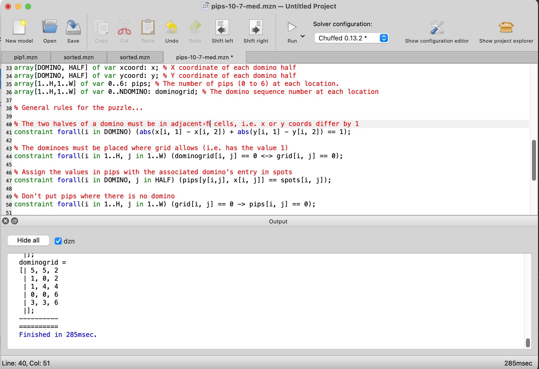
It turned out to find the unique solution in 109 milliseconds, printing out the
solution arrays.
The pips array shows the number of pips in each position, while the dominogrid array shows which
domino (1 through 4) is in each position.
pips =
[| 4, 2, 0
 | 4, 5, 3
 | 1, 1, 1
 |];
dominogrid =
[| 3, 3, 0
 | 2, 1, 4
 | 2, 1, 4
 |];
The text-based solution above is a bit ugly. But it is easy to create graphical output. MiniZinc provides a JavaScript API, so you can easily display solutions on a web page. I wrote a few lines of JavaScript to draw the solution, as shown below. (I just display the numbers since I was too lazy to draw the dots.) Solving this puzzle is not too impressive—it's an "easy" puzzle after all—but I'll show below that the solver can also handle considerably more difficult puzzles.
Graphical display of the solution.
Details of the code
While the above code specifies a particular puzzle, a bit more code is required to define how dominoes and the grid interact. This code may appear strange because it is implemented as constraints, rather than the procedural operations in a normal program.
My main design decision was how to specify the locations of dominoes.
I considered assigning a grid position and orientation
to each domino, but it seemed inconvenient to deal with multiple orientations.
Instead, I decided to position each half of the domino independently, with an x and y coordinate in
the grid.2 I added a constraint that the two halves of each domino had to be in neighboring cells,
that is, either the X or Y coordinates had to differ by 1.
constraint forall(i in DOMINO) (abs(x[i, 1] - x[i, 2]) + abs(y[i, 1] - y[i, 2]) == 1);
It took a bit of thought to fill in the pips array with the number of spots on each domino.
In a normal programming language, one would loop over the dominoes and store the values into pips.
However, here it is done with a constraint so the solver makes sure the values are assigned.
Specifically, for each half-domino, the pips array entry at
the domino's x/y coordinate must equal the corresponding spots on the domino:
constraint forall(i in DOMINO, j in HALF) (pips[y[i,j], x[i, j]] == spots[i, j]);
I decided to add another array to keep track of which domino is in which position.
This array is useful to see the domino locations in the output, but it also
keeps dominoes from overlapping.
I used a constraint to put each domino's number (1, 2, 3, etc.) into the occupied position of dominogrid:
constraint forall(i in DOMINO, j in HALF) (dominogrid[y[i,j], x[i, j]] == i);
Next, how do we make sure that dominoes only go into positions allowed by grid?
I used a constraint that a square in dominogrid must be empty or the corresponding grid must allow a domino.3
This uses the "or" condition, which is expressed as \/, an unusual stylistic
choice. (Likewise, "and" is expressed as /\. These correspond to the logical symbols
∨ and ∧.)
constraint forall(i in 1..H, j in 1..W) (dominogrid[i, j] == 0 \/ grid[i, j] != 0);
Honestly, I was worried that I had too many arrays and the solver would end up in a rathole ensuring that the arrays were consistent. But I figured I'd try this brute-force approach and see if it worked. It turns out that it worked for the most part, so I didn't need to do anything more clever.
Finally, the program requires a few lines to define some constants and variables. The constants below define the number of dominoes and the size of the grid for a particular problem:
int: NDOMINO = 4; % Number of dominoes in the puzzle
int: W = 3; % Width of the grid in this puzzle
int: H = 3; % Height of the grid in this puzzle
Next, datatypes are defined to specify the allowable values.
This is very important for the solver; it is a "finite domain" solver, so limiting the size of
the domains reduces the size of the problem.
For this problem, the values are integers in a particular range, called a set:
set of int: DOMINO = 1..NDOMINO; % Dominoes are numbered 1 to NDOMINO
set of int: HALF = 1..2; % The domino half is 1 or 2
set of int: xcoord = 1..W; % Coordinate into the grid
set of int: ycoord = 1..H;
At last, I define the sizes and types of the various arrays that I use.
One very important syntax is var, which indicates variables that the solver must determine.
Note that the first two arrays, grid and spots do not have var since they are constant,
initialized to specify the problem.
array[1..H,1..W] of 0..1: grid; % The grid defining where dominoes can go
array[DOMINO, HALF] of int: spots; % The number of spots on each half of each domino
array[DOMINO, HALF] of var xcoord: x; % X coordinate of each domino half
array[DOMINO, HALF] of var ycoord: y; % Y coordinate of each domino half
array[1..H,1..W] of var 0..6: pips; % The number of pips (0 to 6) at each location.
array[1..H,1..W] of var 0..NDOMINO: dominogrid; % The domino sequence number at each location
You can find all the code on GitHub.
One weird thing is that because the code is not procedural, the lines can be in any order.
You can use arrays or constants before you use them.
You can even move include statements to the end of the file if you want!
Complications
Overall, the solver was much easier to use than I expected. However, there were a few complications.
By changing a setting, the solver can find multiple solutions instead of stopping after the first. However, when I tried this, the solver generated thousands of meaningless solutions. A closer look showed that the problem was that the solver was putting arbitrary numbers into the "empty" cells, creating valid but pointlessly different solutions. It turns out that I didn't explicitly forbid this, so the sneaky constraint solver went ahead and generated tons of solutions that I didn't want. Adding another constraint fixed the problem. The moral is that even if you think your constraints are clear, solvers are very good at finding unwanted solutions that technically satisfy the constraints. 4
A second problem is that if you do something wrong, the solver simply says that the problem is unsatisfiable. Maybe there's a clever way of debugging, but I ended up removing constraints until the problem can be satisfied, and then see what I did wrong with that constraint. (For instance, I got the array indices backward at one point, making the problem insoluble.)
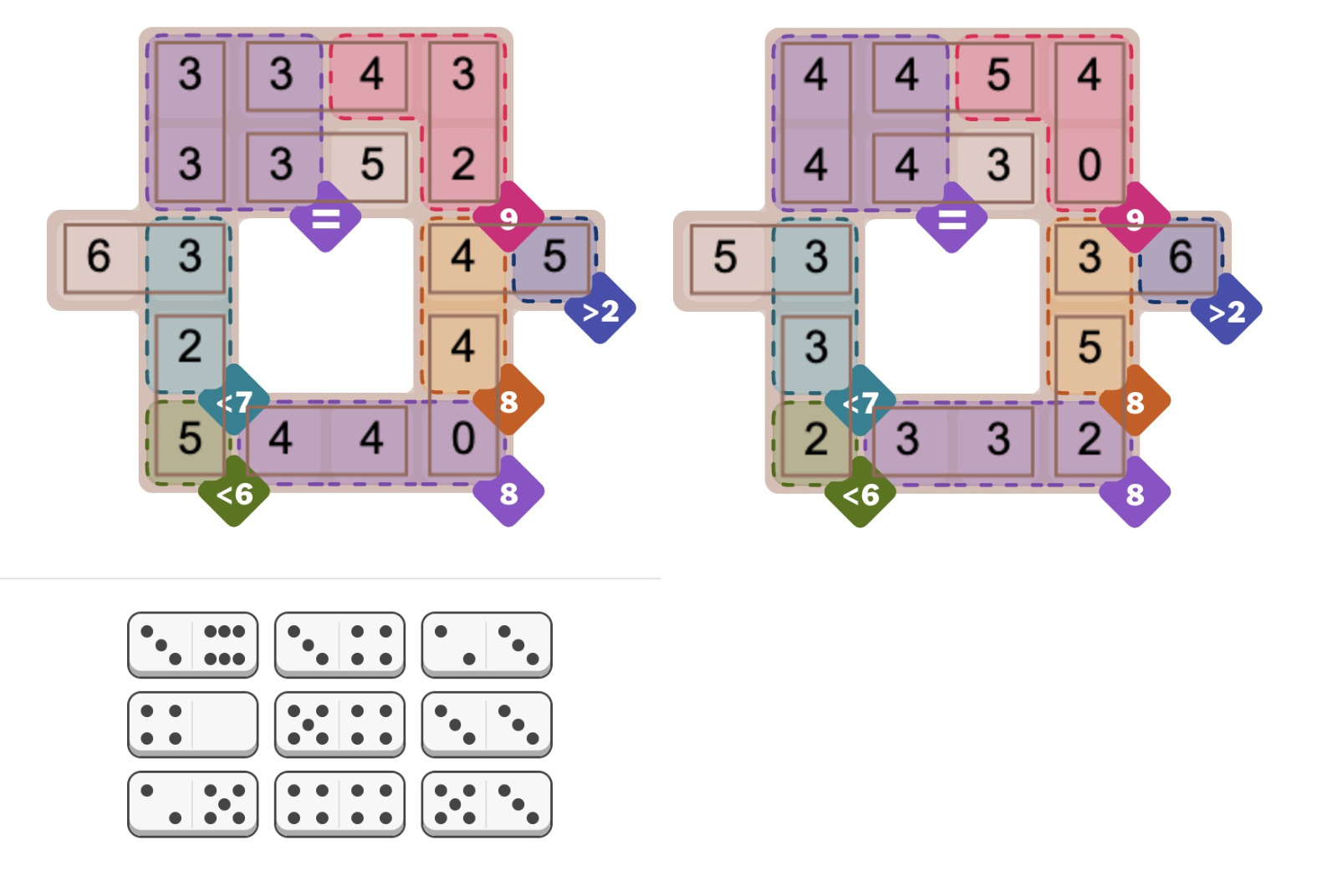
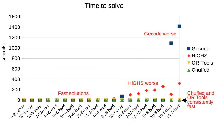
The most concerning issue is the unpredictability of the solver: maybe it will take milliseconds or maybe it will take hours. For instance, the Oct 5 hard Pips puzzle (below) caused the solver to take minutes for no apparent reason. However, the MiniZinc IDE supports different solver backends. I switched from the default Gecode solver to Chuffed, and it immediately found numerous solutions, 384 to be precise. (Sometimes the Pips puzzles sometimes have multiple solutions, which players find controversial.) I suspect that the multiple solutions messed up the Gecode solver somehow, perhaps because it couldn't narrow down a "good" branch in the search tree. For a benchmark of the different solvers, see the footnote.5
Two of the 384 solutions to the NYT Pips puzzle from Oct 5, 2025 (hard difficulty).
How does a constraint solver work?
If you were writing a program to solve Pips from scratch, you'd probably have a loop to try assigning dominoes to positions. The problem is that the problem grows exponentially. If you have 16 dominoes, there are 16 choices for the first domino, 15 choices for the second, and so forth, so about 16! combinations in total, and that's ignoring orientations. You can think of this as a search tree: at the first step, you have 16 branches. For the next step, each branch has 15 sub-branches. Each sub-branch has 14 sub-sub-branches, and so forth.
An easy optimization is to check the constraints after each domino is added. For instance, as soon as the "less than 5" constraint is violated, you can backtrack and skip that entire section of the tree. In this way, only a subset of the tree needs to be searched; the number of branches will be large, but hopefully manageable.
A constraint solver works similarly, but in a more abstract way. The constraint solver assigns values to the variables, backtracking when a conflict is detected. Since the underlying problem is typically NP-complete, the solver uses heuristics to attempt to improve performance. For instance, variables can be assigned in different orders. The solver attempts to generate conflicts as soon as possible so large pieces of the search tree can be pruned sooner rather than later. (In the domino case, this corresponds to placing dominoes in places with the tightest constraints, rather than scattering them around the puzzle in "easy" spots.)
Another technique is constraint propagation. The idea is that you can derive new constraints and catch conflicts earlier. For instance, suppose you have a problem with the constraints "a equals c" and "b equals c". If you assign "a=1" and "b=2", you won't find a conflict until later, when you try to find a value for "c". But with constraint propagation, you can derive a new constraint "a equals b", and the problem will turn up immediately. (Solvers handle more complicated constraint propagation, such as inequalities.) The tradeoff is that generating new constraints takes time and makes the problem larger, so constraint propagation can make the solver slower. Thus, heuristics are used to decide when to apply constraint propagation.
Researchers are actively developing new algorithms, heuristics, and optimizations6 such as backtracking more aggressively (called "backjumping"), keeping track of failing variable assignments (called "nogoods"), and leveraging Boolean SAT (satisfiability) solvers. Solvers compete in annual challenges to test these techniques against each other. The nice thing about a constraint solver is that you don't need to know anything about these techniques; they are applied automatically.
Conclusions
I hope this has convinced you that constraint solvers are interesting, not too scary, and can solve real problems with little effort. Even as a beginner, I was able to get started with MiniZinc quickly. (I read half the tutorial and then jumped into programming.)
One reason to look at constraint solvers is that they are a completely different programming paradigm. Using a constraint solver is like programming on a higher level, not worrying about how the problem gets solved or what algorithm gets used. Moreover, analyzing a problem in terms of constraints is a different way of thinking about algorithms. Some of the time it's frustrating when you can't use familiar constructs such as loops and assignments, but it expands your horizons.
Finally, writing code to solve Pips is more fun than solving the problems by hand, at least in my opinion, so give it a try!
For more, follow me on Bluesky (@righto.com), Mastodon (@[email protected]), RSS, or subscribe here.
all_equal and alldifferent constraint functions.Notes and references
-
I started by downloading the MiniZinc IDE and reading the MiniZinc tutorial. The MiniZinc IDE is straightforward, with an editor window at the top and an output window at the bottom. Clicking the "Run" button causes it to generate a solution.
Screenshot of the MiniZinc IDE. Click for a larger view.
Screenshot of the MiniZinc IDE. Click for a larger view. -
It might be cleaner to combine the X and Y coordinates into a single
Pointtype, using a MiniZinc record type. ↩ -
I later decided that it made more sense to enforce that
dominogridis empty if and only ifgridis 0 at that point, although it doesn't affect the solution. This constraint uses the "if and only if" operator<->.constraint forall(i in 1..H, j in 1..W) (dominogrid[i, j] == 0 <-> grid[i, j] == 0);
↩ -
To prevent the solver from putting arbitrary numbers in the unused positions of
pips, I added a constraint to force these values to be zero:constraint forall(i in 1..H, j in 1..W) (grid[i, j] == 0 -> pips[i, j] == 0);
Generating multiple solutions had a second issue, which I expected: A symmetric domino can be placed in two redundant ways. For instance, a double-six domino can be flipped to produce a solution that is technically different but looks the same. I fixed this by adding constraints for each symmetric domino to allow only one of the two redundant positions. The constraint below forces a preferred orientation for symmetric dominoes.
constraint forall(i in DOMINO) (spots[i,1] != spots[i,2] \/ x[i,1] > x[i,2] \/ (x[i,1] == x[i,2] /\ y[i,1] > y[i,2]));
To enable multiple solutions in MiniZinc, the setting is under Show Configuration Editor > User Defined Behavior > Satisfaction Problems or the
--allflag from the command line. ↩ -
MiniZinc has five solvers that can solve this sort of integer problem: Chuffed, OR Tools CP-SAT, Gecode, HiGHS, and Coin-OR BC. I measured the performance of the five solvers against 20 different Pips puzzles. Most of the solvers found solutions in under a second, most of the time, but there is a lot of variation.
Timings for different solvers on 20 Pip puzzles.
Timings for different solvers on 20 Pip puzzles.Overall, Chuffed had the best performance on the puzzles that I tested, taking well under a second. Google's OR-Tools won all the categories in the 2025 MiniZinc challenge, but it was considerably slower than Chuffed for my Pips programs. The default Gecode solver performed very well most of the time, but it did terribly on a few problems, taking over 15 minutes. HiGHs was slower in general, taking a few minutes on the hardest problems, but it didn't fail as badly as Gecode. (Curiously, Gecode and HiGHS sometimes found different problems to be difficult.) Finally, Coin-OR BC was uniformly bad; at best it took a few seconds, but one puzzle took almost two hours and others weren't solved before I gave up after two hours. (I left Coin-OR BC off the graph because it messed up the scale.)
Don't treat these results too seriously because different solvers are optimized for different purposes. (In particular, Coin-OR BC is designed for linear problems.) But the results demonstrate the unpredictability of solvers: maybe you get a solution in a second and maybe you get a solution in hours. ↩
-
If you want to read more about solvers, Constraint Satisfaction Problems is an overview presentation. The Gecode algorithms are described in a nice technical report: Constraint Programming Algorithms used in Gecode. Chuffed is more complicated: "Chuffed is a state of the art lazy clause solver designed from the ground up with lazy clause generation in mind. Lazy clause generation is a hybrid approach to constraint solving that combines features of finite domain propagation and Boolean satisfiability." The Chuffed paper Lazy clause generation reengineered and slides are more of a challenge. ↩
The Pentium contains a complicated circuit to multiply by three
In 1993, Intel released the high-performance Pentium processor, the start of the long-running Pentium line. I've been examining the Pentium's circuitry in detail and I came across a circuit to multiply by three, a complex circuit with thousands of transistors. Why does the Pentium have a circuit to multiply specifically by three? Why is it so complicated? In this article, I examine this multiplier—which I'll call the ×3 circuit—and explain its purpose and how it is implemented.
It turns out that this multiplier is a small part of the Pentium's floating-point multiplier circuit. In particular, the Pentium multiplies two 64-bit numbers using base-8 multiplication, which is faster than binary multiplication.1 However, multiplying by 3 needs to be handled as a special case. Moreover, since the rest of the multiplication process can't start until the multiplication by 3 finishes, this circuit must be very fast. If you've studied digital design, you may have heard of techniques such as carry lookahead, Kogge-Stone addition, and carry-select addition. I'll explain how the ×3 circuit combines all these techniques to maximize performance.
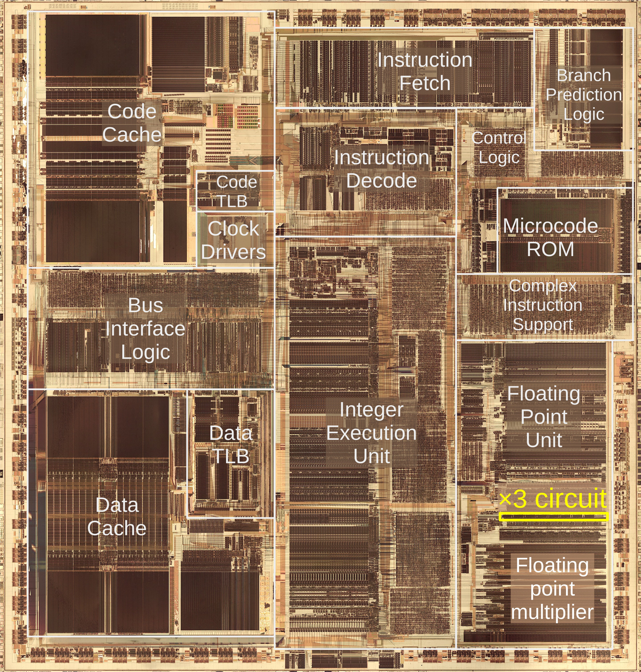
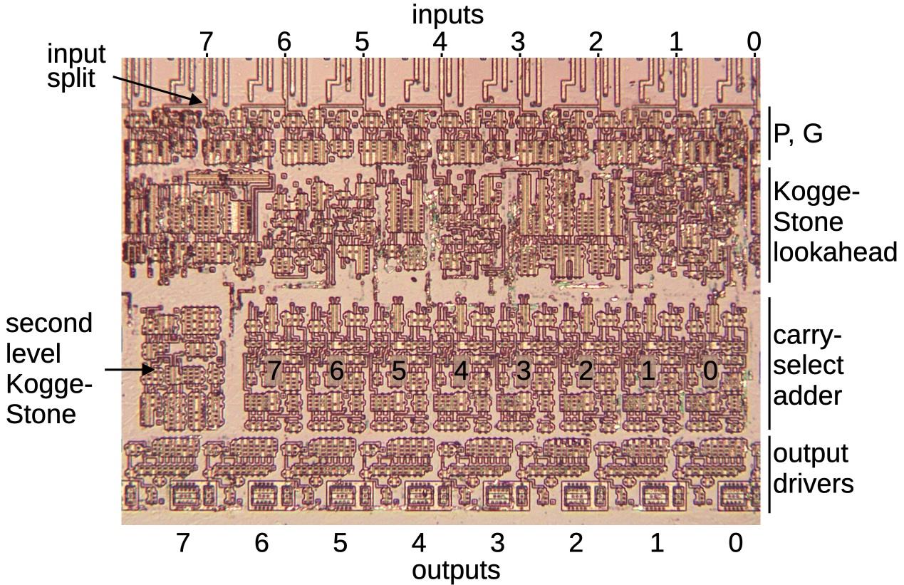
The photo below shows the Pentium's thumbnail-sized silicon die under a microscope. I've labeled the main functional blocks. In the center is the integer execution unit that performs most instructions. On the left, the code and data caches improve memory performance. The floating point unit, in the lower right, performs floating point operations. Almost half of the floating point unit is occupied by the multiplier, which uses an array of adders to rapidly multiply two 64-bit numbers. The focus of this article is the ×3 circuit, highlighted in yellow near the top of the multiplier. As you can see, the ×3 circuit takes up a nontrivial amount of the Pentium die, especially considering that its task seems simple.
This die photo of the Pentium shows the location of the multiplier.
Why does the Pentium use base-8 to multiply numbers?
Multiplying two numbers in binary is conceptually straightforward. You can think of binary multiplication as similar to grade-school long multiplication, but with binary numbers instead of decimal numbers. The example below shows how 5×6 is computed in binary: the three terms are added to produce the result. Conveniently, each term is either the multiplicand (101 in this case) or 0, shifted appropriately, so computing the terms is easy.
 101
 ×110
 ―――
 000 i.e. 0×101
 101 i.e. 1×101
 +101 i.e. 1×101
 ―――――
 11110
Unfortunately, this straightforward multiplication approach is slow. With the three-bit numbers above, there are three terms to add. But if you multiply two 64-bit numbers, you have 64 terms to add, requiring a lot of time and/or circuitry.
The Pentium uses a more complicated approach, computing multiplication in base 8. The idea is to consider the multiplier in groups of three bits, so instead of multiplying by 0 or 1 in each step, you multiply by a number from 0 to 7. Each term that gets added is still in binary, but the number of terms is reduced by a factor of three. Thus, instead of adding 64 terms, you add 22 terms, providing a substantial reduction in the circuitry required. (I'll describe the full details of the Pentium multiplier in a future article.2 )
The downside to radix-8 multiplication is that multiplying by a number from 0 to 7 is much more complicated than multiplying by 0 or 1, which is almost trivial. Fortunately, there are some shortcuts. Note that multiplying by 2 is the same as shifting the number to the left by 1 bit position, which is very easy in hardware—you wire each bit one position to the left. Similarly, to multiply by 4, shift the multiplicand two bit positions to the left.
Multiplying by 7 seems inconvenient, but there is a trick, known as Booth's multiplication algorithm. Instead of multiplying by 7, you add 8 times the number and subtract the number, ending up with 7 times the number. You might think this requires two steps, but the trick is to multiply by one more in the (base-8) digit to the left, so you get the factor of 8 without an additional step. (A base-10 analogy is that if you want to multiply by 19, you can multiply by 20 and subtract the multiplicand.) Thus, you can get the ×7 by subtracting. Similarly, for a ×6 term, you can subtract a ×2 multiple and add ×8 in the next digit. Thus, the only difficult multiple is ×3. (What about ×5? If you can compute ×3, you can subtract that from ×8 to get ×5.)
To summarize, the Pentium's radix-8 Booth's algorithm is a fast way to multiply, but it requires a special circuit to produce the ×3 multiple of the multiplicand.
Implementing a fast ×3 circuit with carry lookahead
Multiplying a number by three is straightforward in binary: add the number to itself, shifted to the left one position. (As mentioned above, shifting to the left is the same as multiplying by two and is easy in hardware.) Unfortunately, using a simple adder is too slow.
The problem with addition is that carries make addition slow. Consider calculating 99999+1 by hand. You'll start with 9+1=10, then carry the one, generating another carry, which generates another carry, and so forth, until you go through all the digits. Computer addition has the same problem: If you're adding two numbers, the low-order bits can generate a carry that then propagates through all the bits. An adder that works this way—known as a ripple carry adder—will be slow because the carry has to ripple through all the bits. As a result, CPUs use special circuits to make addition faster.
One solution is the carry-lookahead adder. In this adder, all the carry bits are computed in parallel, before computing the sums. Then, the sum bits can be computed in parallel, using the carry bits. As a result, the addition can be completed quickly, without waiting for the carries to ripple through the entire sum.
It may seem impossible to compute the carries without computing the sum first, but there's a way to do it.
For each bit position, you determine signals called "carry generate" and "carry propagate".
These signals can then be used to determine all the carries in parallel.
The generate signal indicates that the position generates a carry. For instance, if you add binary
1xx and 1xx (where x is an arbitrary bit), a carry will be generated from the top bit,
regardless of the unspecified bits.
On the other hand, adding 0xx and 0xx will never generate a carry.
Thus, the generate signal is produced for the first case but not the second.
But what about 1xx plus 0xx? We might get a carry, for instance, 111+001, but we might not,
for instance, 101+001. In this "maybe" case, we set the carry propagate signal, indicating that a carry into the
position will get propagated out of the position. For example, if there is a carry out of
the middle position, 1xx+0xx will have a carry from the top bit. But if there is no carry out of the middle position, then
there will not be a carry from the top bit. In other words, the propagate signal indicates that a carry into the top bit will be propagated out of the top
bit.
To summarize, adding 1+1 will generate a carry. Adding 0+1 or 1+0 will propagate a
carry.
Thus, the generate signal is formed at each position by Gn = An·Bn, where A and B are the inputs.
The propagate signal is Pn = An+Bn,
the logical-OR of the inputs.3
Now that the propagate and generate signals are defined, some moderately complex logic4 can compute the carry Cn into each bit position. The important thing is that all the carry bits can be computed in parallel, without waiting for the carry to ripple through each bit position. Once each carry is computed, the sum bits can be computed in parallel: Sn = An ⊕ Bn ⊕ Cn. In other words, the two input bits and the computed carry are combined with exclusive-or. Thus, the entire sum can be computed in parallel by using carry lookahead. However, there are complications.
Implementing carry lookahead with a parallel prefix adder
The carry bits can be generated directly from the G and P signals. However, the straightforward approach requires too much hardware as the number of bits increases. Moreover, this approach needs gates with many inputs, which are slow for electrical reasons. For these reasons, the Pentium uses two techniques to keep the hardware requirements for carry lookahead tractable. First, it uses a "parallel prefix adder" algorithm for carry lookahead across 8-bit chunks.7 Second, it uses a two-level hierarchical approach for carry lookahead: the upper carry-lookahead circuit handles eight 8-bit chunks, using the same 8-bit algorithm.5
The photo below shows the complete ×3 circuit; you can see that the circuitry is divided into blocks of 8 bits. (Although I'm calling this a 64-bit circuit, it really produces a 69-bit output: there are 5 "extra" bits on the left to avoid overflow and to provide additional bits for rounding.)
The full ×3 adder circuit under a microscope.
The idea of the parallel-prefix adder is to
produce the propagate and generate signals across ranges of bits, not just single bits as before.
For instance, the propagate signal P32 indicates that a carry in to bit 2 would be propagated out of bit 3,
(This would happen with 10xx+01xx, for example.)
And G30 indicates that bits 3 to 0 generate a carry out of bit 3.
(This would happen with 1011+0111, for example.)
Using some mathematical tricks,6 you can take the P and G values for two smaller ranges and merge them into the P and G values for the combined range. For instance, you can start with the P and G values for bits 0 and 1, and produce P10 and G10, the propagate and generate signals describing two bits. These could be merged with P32 and G32 to produce P30 and G30, indicating if a carry is propagated across bits 3-0 or generated by bits 3-0. Note that Gn0 tells us if a carry is generated into bit n+1 from all the lower bits, which is the Cn+1 carry value that we need to compute the final sum. This merging process is more efficient than the "brute force" implementation of the carry-lookahead logic since logic subexpressions can be reused.
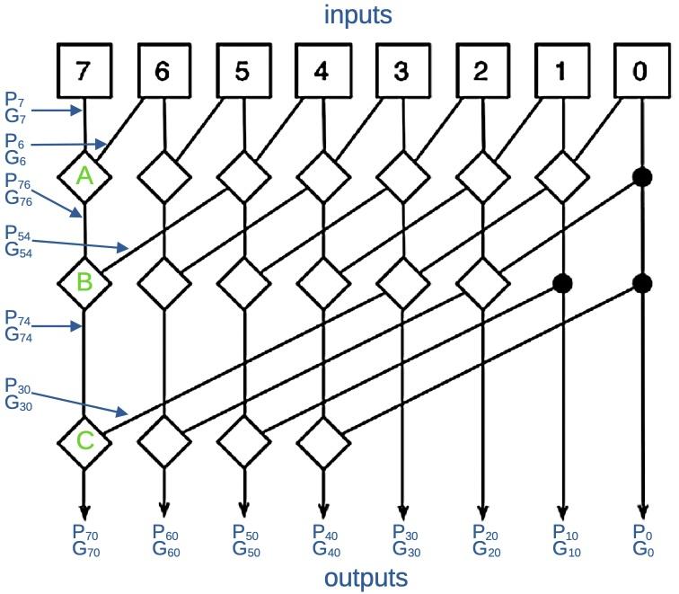
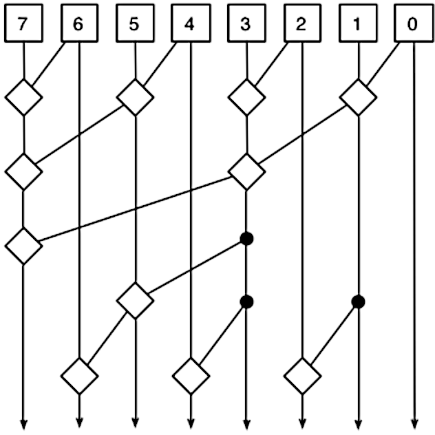
There are many different ways that you can combine the P and G terms to generate the necessary terms.8 The Pentium uses an approach called Kogge-Stone that attempts to minimize the total delay while keeping the amount of circuitry reasonable. The diagram below is the standard diagram that illustrates how a Kogge-Stone adder works. It's rather abstract, but I'll try to explain it. The diagram shows how the P and G signals are merged to produce each output at the bottom. Each square box at the top generates the P and G signals for that bit. Each line corresponds to both the P and the G signal. Each diamond combines two ranges of P and G signals to generate new P and G signals for the combined range. Thus, the signals cover wider ranges of bits as they progress downward, ending with the Gn0 outputs that indicate carries.
I've labeled a few of the intermediate signals so you can get an idea of how it works. Circuit "A" combines P7 and G7 with P6 and G6 to produce the signals describing two bits: P76 and G76. Similarly, circuit "B" combines P76 and G76 with P54 and G54 to produce the signals describing four bits: P74 and G74. Finally, circuit "C" produces the final outputs for bit 7: P70 and G70. Note that most of the intermediate results are used twice, reducing the amount of circuitry. Moreover, there are at most three levels of combination circuitry, reducing the delay compared to a deeper network.
The key point is the P and G values are computed in parallel so the carry bits can all be computed in parallel, without waiting for the carry to ripple through all the bits. (If this explanation doesn't make sense, see my discussion of the Kogge-Stone adder in the Pentium's division circuit for a different—but maybe still confusing—explanation.)
Recursive Kogge-Stone lookahead
The Kogge-Stone approach can be extended to 64 bits, but the amount of circuitry and wiring becomes overwhelming. Instead, the Pentium uses a recursive, hierarchical approach with two levels of Kogge-Stone lookahead. The lower layer uses eight Kogge-Stone adders as described above, supporting 64 bits in total.
The upper layer uses a single eight-bit Kogge-Stone lookahead circuit, treating each of the lower chunks as a single bit. That is, a lower chunk has a propagate signal P indicating that a carry into the chunk will be propagated out, as well as a generate signal G indicating that the chunk generates a carry. The upper Kogge-Stone circuit combines these chunked signals to determine if carries will be generated or propagated by groups of chunks.9
To summarize, each of the eight lower lookahead circuits computes the carries within an 8-bit chunk. The upper lookahead circuit computes the carries into and out of each 8-bit chunk. In combination, the circuits rapidly provide all the carries needed to compute the 64-bit sum.
The carry-select adder
Suppose you're on a game show: "What is 553 + 246 + c? In 10 seconds, I'll tell you if c is 0 or 1 and whoever gives the answer first wins 1000ドル." Obviously, you shouldn't just sit around until you get c. You should do the two sums now, so you can hit the buzzer as soon as c is announced. This is the concept behind the carry-select adder: perform two additions—with a carry-in and without--and then supply the correct answer as soon as the carry is available. The carry-select adder requires additional hardware—two adders along with a multiplexer to select the result—but it overlaps the time to compute the sum with the time to compute the carry. In effect, the addition and the carry lookahead operations are performed in parallel, with the multiplexer combining the results from each.
The Pentium uses a carry-select adder for each 8-bit chunk in the ×3 circuit. The carry from the second-level carry-lookahead selects which sum should be produced for the chunk. Thus, the time to compute the carry is overlapped with the time to compute the sum.
Putting the adder pieces together
The image below zooms in on an 8-bit chunk of the ×3 multiplier, implementing an 8-bit adder. Eight input lines are at the top (along with some unrelated wires). Note that each input line splits with a signal going to the adder on the left and a signal going to the right. This is what causes the adder to multiply by 3: it adds the input and the input shifted one bit to the left, i.e. multiplied by two. The top part of the adder has eight circuits to produce the propagate and generate signals. These signals go into the 8-bit Kogge-Stone lookahead circuit. Although most of the adder consists of a circuit block repeated eight times, the Kogge-Stone circuitry appears chaotic. This is because each bit of the Kogge-Stone circuit is different—higher bits are more complicated to compute than lower bits.
One 8-bit block of the ×3 circuit.
The lower half of the circuit block contains an 8-bit carry-select adder. This circuit produces two sums, with multiplexers selecting the correct sum based on the carry into the block. Note that the carry-select adder blocks are narrower than the other circuitry.10 This makes room for a Kogge-Stone block on the left. The second level Kogge-Stone circuitry is split up; the 8-bit carry-lookahead circuitry has one bit implemented in each block of the adder, and produces the carry-in signal for that adder block. In other words, the image above includes 1/8 of the second-level Kogge-Stone circuit. Finally, eight driver circuits amplify the output bits before they are sent to the rest of the floating-point multiplier.
The block diagram below shows the pieces are combined to form the ×3 multiplier. The multiplier has eight 8-bit adder blocks (green boxes, corresponding to the image above). Each block computes eight bits of the total sum. Each block provides P70 and G70 signals to the second-level lookahead, which determines if each block receives a carry in. The key point to this architecture is that everything is computed in parallel, making the addition fast.
A block diagram of the multiplier.
In the diagram above, the first 8-bit block is expanded to show its contents. The 8-bit lookahead circuit generates the P and G signals that determine the internal carry signals. The carry-select adder contains two 8-bit adders that use the carry lookahead values. As described earlier, one adder assumes that the block's carry-in is 1 and the second assumes the carry-in is 0. When the real carry in value is provided by the second-level lookahead circuit, the multiplexer selects the correct sum.
The photo below shows how the complete multiplier is constructed from 8-bit blocks. The multiplier produces a 69-bit output; there are 5 "extra" bits on the left. Note that the second-level Kogge-Stone blocks are larger on the right than the left since the lookahead circuitry is more complex for higher-order bits.
Going back to the full ×3 circuit above, you can see that the 8 bits on the right have significantly simpler circuitry. Because there is no carry-in to this block, the carry-select circuitry can be omitted. The block's internal carries, generated by the Kogge-Stone lookahead circuitry, are added using exclusive-NOR gates. The diagram below shows the implementation of an XNOR gate, using inverters and a multiplexer.
The XNOR circuit
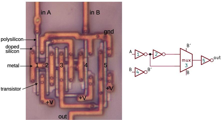
I'll now describe one of the multiplier's circuits at the transistor level, in particular an XNOR gate. It's interesting to look at XNOR because XNOR (like XOR) is a tricky gate to implement and different processors use very different approaches. For instance, the Intel 386 implements XOR from AND-NOR gates (details) while the Z-80 uses pass transistors (details). The Pentium, on the other hand, uses a multiplexer.
An exclusive-NOR gate with the components labeled. This is a focus-stacked image.
The diagram above shows one of the XNOR gates in the adder's low bits.11 The gate is constructed from four inverters and a pass-transistor multiplexer. Input B selects one of the multiplexer's two inputs: input A or input A inverted. The result is the XNOR function. (Inverter 1 buffers the input, inverter 5 buffers the output, and inverter 4 provides the complemented B signal to drive the multiplexer.)
For the photo, I removed the top two metal layers from the chip, leaving the bottom metal layer, called M1. The doped silicon regions are barely visible beneath the metal. When a polysilicon line crosses doped silicon, it forms the gate of a transistor. This CMOS circuit has NMOS transistors at the top and PMOS transistors at the bottom. Each inverter consists of two transistors, while the multiplexer consists of four transistors.
The BiCMOS output drivers
The outputs from the ×3 circuit require high current. In particular, each signal from the ×3 circuit can drive up to 22 terms in the floating-point multiplier. Moreover, the destination circuits can be a significant distance from the ×3 circuit due to the size of the multiplier. Since the ×3 signals are connected to many transistor gates through long wires, the capacitance is high, requiring high current to change the signals quickly.
The Pentium is constructed with a somewhat unusual process called BiCMOS, which combines bipolar transistors and CMOS on the same chip. The Pentium extensively uses BiCMOS circuits since they reduced signal delays by up to 35%. Intel also used BiCMOS for the Pentium Pro, Pentium II, Pentium III, and Xeon processors. However, as chip voltages dropped, the benefit from bipolar transistors dropped too and BiCMOS was eventually abandoned.
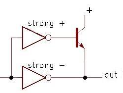
The schematic below shows a simplified BiCMOS driver that inverts its input. A 0 input turns on the upper inverter, providing current into the bipolar (NPN) transistor's base. This turns on the transistor, causing it to pull the output high strongly and rapidly. A 1 input, on the other hand, will stop the current flow through the NPN transistor's base, turning it off. At the same time, the lower inverter will pull the output low. (The NPN transistor can only pull the output high.)
Note the asymmetrical construction of the inverters. Since the upper inverter must provide a large current into the NPN transistor's base, it is designed to produce a strong (high-current) positive output and a weak low output. The lower inverter, on the other hand, is responsible for pulling the output low. Thus, it is constructed to produce a strong low output, while the high output can be weak.
The basic circuit for a BiCMOS driver.
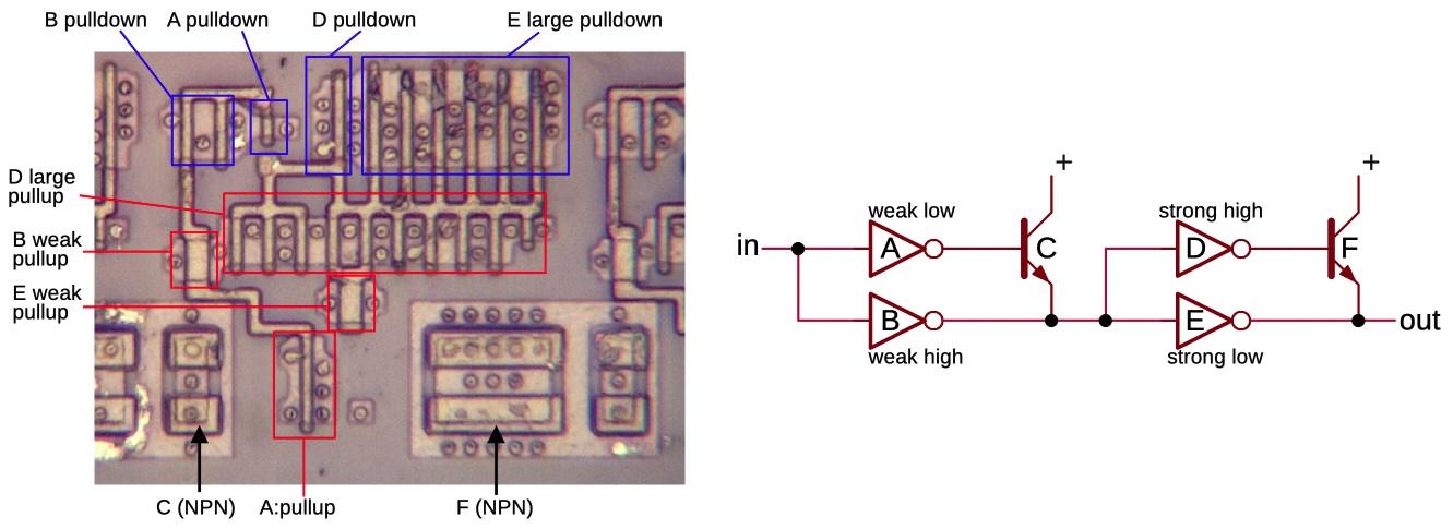
The driver of the ×3 circuit goes one step further: it uses a BiCMOS driver to drive a second BiCMOS driver. The motivation is that the high-current inverters have fairly large transistor gates, so they need to be driven with high current (but not as much as they produce, so there isn't an infinite regress).12
The schematic below shows the BiCMOS driver circuit that the ×3 multiplier uses. Note the large, box-like appearance of the NPN transistors, very different from the regular MOS transistors. Each box contains two NPN transistors sharing collectors: a larger transistor on the left and a smaller one on the right. You might expect these transistors to work together, but the contiguous transistors are part of two separate circuits. Instead, the small NPN transistor to the left and the large NPN transistor to the right are part of the same circuit.
One of the output driver circuits, showing the polysilicon and silicon.
The inverters are constructed as standard CMOS circuits with PMOS transistors to pull the output high and NMOS transistors to pull the output low. The inverters are carefully structured to provide asymmetrical current, making them more interesting than typical inverters. Two pullup transistors have a long gate, making these transistors unusually weak. Other parts of the inverters have multiple transistors in parallel, providing more current. Moreover, the inverters have unusual layouts, with the NMOS and PMOS transistors widely separated to make the layout more efficient. For more on BiCMOS in the Pentium, see my article on interesting BiCMOS circuits in the Pentium.
Conclusions
Hardware support for computer multiplication has a long history going back to the 1950s.13 Early microprocessors, though, had very limited capabilities, so microprocessors such as the 6502 didn't have hardware support for multiplication; users had to implement multiplication in software through shifts and adds. As hardware advanced, processors provided multiplication instructions but they were still slow. For example, the Intel 8086 processor (1978) implemented multiplication in microcode, performing a slow shift-and-add loop internally. Processors became exponentially more powerful over time, as described by Moore's Law, allowing later processors to include dedicated multiplication hardware. The 386 processor (1985) included a multiply unit, but it was still slow, taking up to 41 clock cycles for a multiplication instruction.
By the time of the Pentium (1993), microprocessors contained millions of transistors, opening up new possibilities for design. With a seemingly unlimited number of transistors, chip architects could look at complicated new approaches to squeeze more performance out of a system. This ×3 multiplier contains roughly 9000 transistors, a bit more than an entire Z80 microprocessor (1976). Keep in mind that the ×3 multiplier is a small part of the floating-point multiplier, which is part of the floating-point unit in the Pentium. Thus, this small piece of a feature is more complicated than an entire microprocessor from 17 years earlier, illustrating the incredible growth in processor complexity.
I plan to write more about the implementation of the Pentium, so follow me on Bluesky (@righto.com) or RSS for updates. (I'm no longer on Twitter.) The Pentium Navajo rug inspired me to examine the Pentium in more detail.
Footnotes and references
-
A floating-point multiplication on the Pentium takes three clock cycles, of which the multiplication circuitry is busy for two cycles. (See Agner Fog's optimization manual.) In comparison, integer multiplication (
MUL) is much slower, taking 11 cycles. The Nehalem microarchitecture (2008) reduced floating-point multiplication time to 1 cycle. ↩ -
I'll give a quick outline of the Pentium's floating-point multiplier as a preview. The multiplier is built from a tree of ten carry-save adders to sum the terms. Each carry-save adder is a 4:2 compression adder, taking four input bits and producing two output bits. The output from the carry-save adder is converted to the final result by an adder using Kogge-Stone lookahead and carry select. Multiplying two 64-bit numbers yields 128 bits, but the Pentium produces a 64-bit result. (There are actually a few more bits for rounding.) The low 64 bits can't simply be discarded because they could produce a carry into the preserved bits. Thus, the low 64 bits go into another Kogge-Stone lookahead circuit that doesn't produce a sum, but indicates if there is a carry. Since the datapath is 64 bits wide, but the product is 128 bits, there are many shift stages to move the bits to the right column. Moreover, the adders are somewhat wider than 64 bits as needed to hold the intermediate sums. ↩
-
The bits
1+1will set generate, but should propagate be set too? It doesn't make a difference as far as the equations. This adder sets propagate for1+1but some other adders do not. The answer depends on if you use an inclusive-or or exclusive-or gate to produce the propagate signal. ↩ -
The carry Cn at each bit position n can be computed from the G and P signals by considering the various cases:
C1 = G0: a carry into bit 1 occurs if a carry is generated from bit 0.
C2 = G1 + G0P1: A carry into bit 2 occurs if bit 1 generates a carry or bit 1 propagates a carry from bit 0.
C3 = G2 + G1P2 + G0P1P2: A carry into bit 3 occurs if bit 2 generates a carry, or bit 2 propagates a carry generated from bit 1, or bits 2 and 1 propagate a carry generated from bit 0.
C4 = G3 + G2P3 + G1P2P3 + G0P1P2P3: A carry into bit 4 occurs if a carry is generated from bit 3, 2, 1, or 0 along with the necessary propagate signals.
And so on...Note that the formula gets more complicated for each bit position. The circuit complexity is approximately O(N3), depending on how you measure it. Thus, implementing the carry lookahead formula directly becomes impractical as the number of bits gets large. The Kogge-Stone approach uses approximately O(N log N) transistors, but the wiring becomes excessive for large N since there are N/2 wires of length N/2. Using a tree of Kogge-Stone circuits reduces the amount of wiring. ↩
-
The 8-bit chunks in the circuitry have nothing to do with bytes. The motivation is that 8 bits is a reasonable size for a chunk, as well as providing a nice breakdown into 8 chunks of 8 bits. Other systems have used 4-bit chunks for carry lookahead (such as minicomputers based on the 74181 ALU chip). ↩
-
I won't go into the mathematics of merging P and G signals; see, for example, Adder Circuits or Carry Lookahead Adders for additional details. The important factor is that the carry merge operator is associative (actually a monoid), so the sub-ranges can be merged in any order. This flexibility is what allows different algorithms with different tradeoffs. ↩
-
The idea behind a prefix adder is that we want to see if there is a carry out of bit 0, bits 0-1, bits 0-2, bits 0-3, 0-4, and so forth. These are all the prefixes of the word. Since the prefixes are computed in parallel, it's called a parallel prefix adder. ↩
-
The lookahead merging process can be implemented in many ways, including Kogge-Stone, Brent-Kung, and Ladner-Fischer, with different tradeoffs. For one example, the diagram below shows that Brent-Kung uses fewer "diamonds" but more layers. Thus, a Brent-Kung adder uses less circuitry but is slower. (You can follow each output upward to verify that the tree reaches the correct inputs.)
A diagram of an 8-bit Brent-Kung adder. Diagram by Robey Pointer, Wikimedia Commons.
A diagram of an 8-bit Brent-Kung adder. Diagram by Robey Pointer, Wikimedia Commons. -
The higher-level Kogge-Stone lookahead circuit uses the eight P70 and G70 signals from the eight lower-level lookahead circuits. Note that P70 and G70 indicate that an 8-bit chunk will propagate or generate a carry. The higher-level lookahead circuit treats 8-bit chunks as a unit, while the lower-level lookahead circuit treats 1-bit chunks as a unit. Thus, the higher-level and lower-level lookahead circuits are essentially identical, acting on 8-bit values. ↩
-
The floating-point unit is built from fixed-width columns, one for each bit. Each column is 38.5 μm wide, so the circuitry in each column must be designed to fit that width. For the most part, the same circuitry is repeated for each of the 64 (or so) bits. The carry-select adder is unusual since it doesn't follow the column width of the rest of the floating-point unit. Instead, it crams 8 circuits into the width of 6.5 regular circuits. This leaves room for one Kogge-Stone circuitry block. ↩
-
Because there is no carry-in to the lowest 8-bit block of the ×3 circuit, the carry-select circuit is not needed. Instead, each output bit can be computed using an XNOR gate. ↩
-
The principle of Logical Effort explains that for best performance, you don't want to jump from a small signal to a high-current signal in one step. Instead, a small signal produces a medium signal, which produces a larger signal. By using multiple stages of circuitry, the overall delay can be reduced. ↩
-
The Booth multiplication technique was described in 1951, while parallel multipliers were proposed in the mid-1960s by Wallace and Dadda. Jumping ahead to higher-radix multiplication, a 1992 paper A Fast Hybrid Multiplier Combining Booth and Wallace/Dadda Algorithms from Motorola discusses radix-4 and radix-8 algorithms for a 32-bit multiplier, but decides that computing the ×3 multiple makes radix-8 impractical. IBM discussed a 32-bit multiplier in 1997: A Radix-8 CMOS S/390 Multiplier. Bewick's 1994 PhD thesis Fast Multiplication: Algorithms and Implementation describes numerous algorithms.
For adders, Two-Operand Addition is an interesting presentation on different approaches. CMOS VLSI Design has a good discussion of addition and various lookahead networks. It summarizes the tradeoffs: "Brent-Kung has too many logic levels. Sklansky has too much fanout. And Kogge-Stone has too many wires. Between these three extremes, the Han-Carlson, Ladner-Fischer, and Knowles trees fill out the design space with different compromises between number of stages, fanout, and wire count." The approach used in the Pentium's ×3 multiplier is sometimes called a sparse-tree adder. ↩
Qui-binary arithmetic: how a 1960s IBM mainframe does math
The IBM 1401 computer uses an unusual technique called qui-binary arithmetic to perform arithmetic. In the early 1960s, the IBM 1401 was the most popular computer, used by many businesses for the low monthly price of 2500ドル. For a business computer, error detection was critical: if a company sent out bad payroll checks because of a hardware fault, it would be catastrophic. By using qui-binary arithmetic, the IBM 1401 detects arithmetic errors.
If you've studied digital circuits, you've seen the standard binary adder circuits that add two numbers. But the IBM 1401 uses a totally different approach. Unlike modern computers, the IBM 1401 operates on decimal digits, not binary numbers, using BCD (binary-coded decimal). To add two numbers, digits are converted from BCD to qui-binary, added together with a special qui-binary adder, and then converted back to digits in BCD. This may seem pointlessly complex, but it allows easy error detection.
The photo below shows the IBM 1401 with one panel opened to show the addition/subtraction circuitry, made up of dozens of Standard Module System (SMS) cards. Each SMS card holds a simple circuit with a few germanium transistors (the computer predates silicon transistors). This article explains in detail how these circuits implement it.
What is qui-binary?
Qui-binary code is a way of representing a decimal digit with 7 bits. The number is split into a qui part (0, 2, 4, 6, or 8) and a binary part (0 or 1).[1] For example, 3 is split into 2+1, and 8 is split into 8+0. The qui part is labeled Q0, Q2, Q4, Q6, or Q8 and the binary part is B0 or B1. The number is then represented by seven bits: Q8Q6Q4Q2Q0B1B0. The following table summarizes the qui-binary representation.
| Digit | Qui | Binary | Bits: Q8Q6Q4Q2Q0B1B0 |
|---|---|---|---|
| 0 | Q0 | B0 | 0000101 |
| 1 | Q0 | B1 | 0000110 |
| 2 | Q2 | B0 | 0001001 |
| 3 | Q2 | B1 | 0001010 |
| 4 | Q4 | B0 | 0010001 |
| 5 | Q4 | B1 | 0010010 |
| 6 | Q6 | B0 | 0100001 |
| 7 | Q6 | B1 | 0100010 |
| 8 | Q8 | B0 | 1000001 |
| 9 | Q8 | B1 | 1000010 |
The advantage of qui-binary is error detection, since it is straightforward to detect an invalid qui-binary number.[2] A valid qui-binary number has exactly one qui bit and exactly one binary bit. Any other qui-binary number is faulty. For instance, Q4 Q2 B0 is bad, as is Q8. A problem in any bit creates a bad qui-binary number and can be detected.
Overview of the 1401's qui-binary circuit
The IBM 1401's arithmetic unit operates on one digit at a time, adding them with a qui-binary adder.[3] The block diagram below[4] shows how the adder takes two binary-coded decimal digits, stored in the A and B temporary registers, and produces their sum. The digit from the A register enters on the left, and is translated to qui-binary by the translation circuit (labeled XLATOR). This qui-binary value goes through a translate/complement circuit which is used for subtraction. The digit in the B register enters on the right and is also converted to qui-binary. The binary bits (B0/B1) are added by the binary adder at the bottom. The quinary values are added with a special quinary adder. The adder output circuit combines the quinary bits with any carry, generating the qui-binary result. Finally, the translation circuit at the top converts the qui-binary result back to a BCD digit, sending the BCD value to core memory and to the console display lights.[5]
Overview of the arithmetic unit in the IBM 1401 mainframe.
The photo below shows the IBM 1401 console during an addition instruction. The numbers are displayed in binary-coded decimal; the qui-binary representation is entirely hidden from the programmer. At this point in the addition instruction, the digit 1 was read from address 423 into the B register, and is added to the digit 2 already in the A register. The result from the qui-binary adder is 3 (binary 2 + 1), which is stored back to memory.[6]
The IBM 1401 console, showing an addition operation.
BCD to qui-binary translation
To examine the addition/subtraction circuitry in more detail, we'll start with the logic that converts a BCD digit to qui-binary. The logic is implement with an AND-OR structure that is common in the 1401. Note that the logic gate symbols are different from modern symbols: an AND gate is represented as a triangle, and an OR gate is represented as a semi-circle. Each bit of the BCD digit, as well as the bit's complement, is provided as input. Each AND gate matches a specific bit pattern, and then the results are combined with an OR gate to generate an output.The circuit in an IBM 1401 mainframe to translate a BCD digit into qui-binary code.
To see how this works, look at the AND gate at the bottom (labeled 8, 9). Tracing the wires to the inputs, this gate will be active if input 8 AND input not-4 AND input not-2 are set, i.e. if the input is binary 1000 or 1001. Thus, output Q8 will be set if the input digit is 8 or 9, just as required for the qui-binary code.
For a slightly more complicated case, the first AND gate matches binary 1010 (decimal 10), and the second AND gate matches binary 000x (decimal 0 or 1). Thus, Q0 will be set for inputs 0, 1, or 10. Likewise, Q2 is set for inputs 2, 3, or 11. The other Q outputs are simpler, computed with a single AND gate.[7]
The B0 and B1 outputs are simply wires from the not-1 and 1 inputs. If the input is even, B0 is set, and if the input is odd, B1 is set.
9's complement circuit
To perform subtraction, the IBM 1401 adds the 9's complement of the digit. The 9's complement is simply 9 minus the digit. The complement circuit below passes the qui-binary number through unchanged for addition or complemented for subtraction.[8] The complement input selects which mode to use; it is generated from the operation (addition or subtraction), and the signs of the input numbers.To see how complementation works in qui-binary, consider 3 (Q2 B1). Its complement is 6 (Q6 B0). The general pattern for complementation is B0 and B1 get swapped. Q0 and Q8 are swapped, and Q2 and Q6 are swapped. Q4 is unchanged; for example, 4 (Q4 B0) is complemented to 5 (Q4 B1).[9]
Quinary adder
The circuit below adds the quinary parts of the two numbers and can be considered the "meat" of the adder. The qui part from the A register is on the left, the qui part from the B register is on the top, and the qui output is on the right. The outputs with "+c" indicate a carry if the result is 10 or more. The addition logic is implemented with a "brute force" matrix, connecting each pair of inputs to the appropriate output. An example is Q2 + Q6, shown in red. If these two inputs are set, the indicated AND gate will trigger the Q8 output.[10]
In the photo below, we can find the exact card in the IBM 1401 that performs this addition. The card in the upper left marked with a red asterisk computes the output Q8.[11]
The SMS cards in the IBM 1401 that perform arithmetic.
The circuitry in the IBM 1401 is simple enough that you can follow it all the way to the function of individual transistors.[12] The asterisk-marked card is a 3JMX SMS card containing 4 AND gates, and is shown below. Each of the round metal transistors corresponds to one AND gate for one of the sums that generates the output Q8. The top transistor is activated by inputs 8+0, the next for 0+8, the next 6+2, and the bottom one 2+6. Thus, the bottom transistor corresponds to the red AND gate in the schematic above.[13]
The SMS card of type 3JMX has four AND gates.
Qui-binary to BCD translation
The diagram below shows the remainder of the qui-binary adder, which combines the qui and binary parts of the output, converts the output back to BCD, and detects errors. I'll just give an overview here, with more explanation in the footnotes.[14] The qui-binary carry circuit, in the blue box, processes the carry signals from the adder circuit. The next circuit, in the green box, applies any carry from the B bits, incrementing the qui component if necessary. The translation circuit, in red, converts the qui-binary result to BCD, using AND-OR logic. It also generates the parity output used for error detection in memory. The final circuit, in purple, is the error detection circuit which verifies the qui-binary result is valid and halts the computer if there is a fault.The circuitry in the IBM 1401 mainframe to convert a qui-binary sum to a BCD result.
The photo below shows the functions of the different cards in the arithmetic rack.[15] The cards in the left half perform arithmetic operations. Each function takes multiple cards, since a single SMS card has a small amount of circuitry. "Q8" indicates the card discussed earlier that computes Q8. The right half is taken up with clock and timing circuits, which generate the clock signals that control the 1401.
Conclusion
This article has discussed how the 1401 adds or subtracts a single digit. The complete addition/subtraction process in the 1401 is even more complex because the 1401 handles numbers of arbitrary length; the hardware loops over each digit to process the entire numbers.[16] [17]Studying old computers such as the IBM 1401 is interesting because they use unusual, forgotten techniques such as qui-binary arithmetic. While qui-binary arithmetic seems strange at first, its error-detection properties made it useful for the IBM 1401. Old computers are also worth studying because their circuitry can be thoroughly understood. After careful examination, you can see how arithmetic, for instance, works, down to the function of individual transistors.
Thanks to the 1401 restoration team and the Computer History Museum for their assistance with this article. The IBM 1401 is regularly demonstrated at the Computer History Museum, usually on Wednesdays and Saturdays (schedule), so check it out if you're in Silicon Valley.
Notes and references
[1] Qui-binary is the opposite of bi-quinay encoding used in abacuses and old computers such as the IBM 650. In bi-quinary, the bi part is 0 or 5, and the quinary part is 0, 1, 2, 3, or 4.[2] You might wonder why IBM didn't just use parity instead of qui-binary numbers. While parity detects bit errors, it doesn't work well for detecting errors during addition. There's no easy way to figure out what the parity should be for a sum.
[3] The IBM 1401 has hardware to multiply and divide numbers of arbitrary length. The multiplication and division operations are based on repeated addition and subtraction, so they use the qui-binary addition circuit, along with qui-binary doublers.
[4] The logic diagrams are all from the 1401 Instructional Logic Diagrams (ILD). Pages 25 and 26 show the addition and subtraction logic if you want to see the diagrams in context.
[5] The IBM 1401 performs operations on memory locations and the A and B registers provide temporary storage for digits as they are read from core memory. They are not general-purpose registers as in most microprocessors.
[6] A few more details about the console display. The "C" bit at the top of each register is the check (parity) bit used for error detection. The 1401 uses odd parity, so if an even number of bits are set, the C bit is also set. The "M" bit at the bottom is the word mark, which indicates the end of a variable-length field. The machine opcode character is zone B + zone A + 1, which indicates the letter "A".
Unlike modern computers, the 1401 uses intuitive opcodes so "A" means add, "S" means subtract, "B" means branch and so forth. (This is the actual opcode in memory, not the assembly mnemonic.) In the lower right, the mode knob is set to "Single cycle process", which allowed me to step through the instruction to get this picture. Normally this knob is set to "Run" and the console flashes frantically as instructions are executed.
[7] One surprising feature of the BCD translator is that it accepts binary inputs from 0 to 15, not just "valid" inputs 0 to 9. Input 10 is treated as 0, since the 1401 stores the digit 0 as decimal 10 in core. Values 11 through 15 are treated as 3 through 7. Thus, every binary input results in a valid (but probably unexpected) qui-binary value. As a result, the 1401 can perform addition on non-decimal characters, but the results aren't very useful.
[8] The IBM 1401 uses 9's complements since it is a decimal machine, unlike modern binary computers which use 2's complements. For example, the complement of 1 is 8, and the complement of 4 is 5. To subtract a number, the 9's complement of each digit is added (along with a carry). An example of using complements for subtration is 432 - 145. The 9's complement of 145 is 854. 432 +たす 854 +たす 1 =わ 1287. Discarding the top digit yields the desired result 432 - 145 = 287. Complements are explained in more detail in Wikipedia.
[9] If you trace through the AND-OR logic in the complement circuit, you can see that each pair of AND gates and and OR gate forms a multiplexer, selecting one input or the other. For example for the B1 output: if complement is 0 AND B1 is 1, the output is 1. OR, if complement is 1 AND B0 is 1, the output is 1. In other words, the output matches the B1 input if complement is 0, and matches the B0 input if complement is 1. The box labeled I in the schematic is an inverter.
[10] The quinary adder is implemented using wired-OR logic. Instead of an explicit OR gate, the AND outputs are simply wired together to produce the OR output. While the quinary adder looks symmetrical and regular in the schematic, its implementation uses three different SMS cards: 3JMX and 4JMX AND/OR gates, and JGVW AND gates, depending on the number of AND gates feeding the output.
[11] One component of interest in the photo of SMS cards is the silver rectangle on the lower right card. This is the quartz crystal that generates timing for the 1401. The SMS card is type RK, and the crystal runs the 347.5kHz oscillator. Eight oscillator half-cycles make up the 11.5 microsecond cycle time of the 1401. At the top of the photo are the wiring bundles connecting these circuits to other parts of the computer.
[12] Due to the simplicity of the IBM 1401 compared to modern computers, it's possible to understand how the IBM 1401 works at every level all the way to quantum physics. I'll give an outline here. The gates in an SMS card use a simple form of logic called CTDL by IBM and DTL (Diode-Transistor Logic) by the rest of the world. The 3JMX card schematic shows that each input is connected through a diode to the output transistor. If any input is high, current flows through the diode and turns off the transistor. The result is an AND gate (with inverted inputs). IBM Transistor Component Circuits (page 108) explains this circuit in detail.
Going deeper, we can look inside the transistor. The board uses type 034 germanium alloy-junction transistors (details, details), very different from modern silicon-based planar transistors. These transistors consist of a germanium crystal base with indium beads fused on either side to form the emitter and collector. The regions of germanium-indium alloy form the "P" regions. In the photo, the germanium disk is in the small circular hole. Copper wires are connected to the indium beads. The photo below shows an IBM 083 transistor from the IBM 1401. This is the NPN version of the transistors in the 3JMX card. If you want a deeper understanding, look at bipolar junction transistor theory, which in turn is explained by quantum physics and solid-state device theory.
[13] You may wonder how 8=4+4 gets computed, since the card described doesn't handle that. The sum 4+4 is computed by the card just below the asterisk (a triple AND gate card of type JGVW). The other two AND gates in that card compute 6+6 and 8+8. To determine what each board in the IBM 1401 does, look at the Automated Logic Diagrams, page 34.32.14.2.
[14] The qui-binary carry logic happens in several phases. The qui parts are added, generating a carry if needed. The binary parts are added with a simple binary adder (not shown). A carry from the binary part shifts the qui part by 2. A carry out signal is also generated as needed. For instance, adding 3 + 5 is done by adding Q2 B1 + Q4 B1. This generates Q6 + B0 + B carry. The B carry increments the qui component to Q8, yielding the result Q8 B0 (i.e. 8).
The qui-binary to BCD translation circuit uses straightforward AND-OR logic, detecting the various combinations. Note that 0 is represented in the 1401 as binary 1010 (because binary 0000 indicates a blank), so the BCD output bits 8 and 2 are set for qui-binary value Q0 B0. The parity output is generate by combining the binary parity (even for B0; odd for B1) with the qui parity value. The qui even parity signal is set for Q0 or Q6, while the qui odd parity signal is set for Q2, Q4, Q8. Note that representing 0 as binary 1010 instead of 0000 doesn't affect the parity.
The error detection circuit uses AND-OR logic to detect bad qui-binary results. It detects a fault if no B bits are set or both B bits are set. Instead of testing every qui bit combination, it implements a short cut from the qui parity circuit. If the even qui parity signal and the odd qui parity signal are both set, this indicates multiple qui lines are set, triggering a fault. If neither qui parity signal is set, then no qui lines are set, also triggering a fault. The parity check misses a few qui combinations (such as Q0 and Q6 set), so these are tested separately. The result is that any invalid qui-binary result triggers a fault.
[15] The rack of cards shown is officially known as gate 01B3. The functions assigned to each card in the photo are approximate, because some cards are used by multiple functions. For exact information, see the plug list, which specifies the card type and function for every card in the 1401.
[16] One complication with the 1401's arithmetic instructions are numbers are stored as a positive value with a sign bit (on the last digit). This format makes printing of positive and negative numbers simpler, which is important for a business computer, but it makes arithmetic more complicated. First, the signs must be checked to determine if the numbers are being added or subtracted. Next, each digit is added or subtracted in sequence until the end of the number is reached. If the result is negative, the 1401 flips the result sign and converts the answer back to a positive value by making two additional digit-by-digit passes over the number. Modern computers use binary and handle negative numbers with two's complement, which makes subtraction much simpler. It takes 9 pages of documentation to explain the addition operation, complete with multiple flowcharts: see IBM 1401 Data Flow pages 24-32. (Keep in mind that these flowcharts are implemented in hardware, not with microcode or subroutines.)
[17] Arithmetic on the 1401 and the qui-binary adder are discussed in detail in 1401 Instruction Logic, pages 49-67. For the history leading up to qui-binary arithmetic, see this article by Carl Claunch.
Mining Bitcoin with pencil and paper: 0.67 hashes per day
A pencil-and-paper round of SHA-256
The mining process
Bitcoin mining is a key part of the security of the Bitcoin system. The idea is that Bitcoin miners group a bunch of Bitcoin transactions into a block, then repeatedly perform a cryptographic operation called hashing zillions of times until someone finds a special extremely rare hash value. At this point, the block has been mined and becomes part of the Bitcoin block chain. The hashing task itself doesn't accomplish anything useful in itself, but because finding a successful block is so difficult, it ensures that no individual has the resources to take over the Bitcoin system. For more details on mining, see my Bitcoin mining article.A cryptographic hash function takes a block of input data and creates a smaller, unpredictable output. The hash function is designed so there's no "short cut" to get the desired output - you just have to keep hashing blocks until you find one by brute force that works. For Bitcoin, the hash function is a function called SHA-256. To provide additional security, Bitcoin applies the SHA-256 function twice, a process known as double-SHA-256.
In Bitcoin, a successful hash is one that starts with enough zeros.[1] Just as it is rare to find a phone number or license plate ending in multiple zeros, it is rare to find a hash starting with multiple zeros. But Bitcoin is exponentially harder. Currently, a successful hash must start with approximately 17 zeros, so only one out of 1.4x10²⁰ hashes will be successful. In other words, finding a successful hash is harder than finding a particular grain of sand out of all the grains of sand on Earth.
The following diagram shows a block in the Bitcoin blockchain along with its hash. The yellow bytes are hashed to generate the block hash. In this case, the resulting hash starts with enough zeros so mining was successful. However, the hash will almost always be unsuccessful. In that case, the miner changes the nonce value or other block contents and tries again.
The SHA-256 hash algorithm used by Bitcoin
The SHA-256 hash algorithm takes input blocks of 512 bits (i.e. 64 bytes), combines the data cryptographically, and generates a 256-bit (32 byte) output. The SHA-256 algorithm consists of a relatively simple round repeated 64 times. The diagram below shows one round, which takes eight 4-byte inputs, A through H, performs a few operations, and generates new values of A through H.
The blue boxes mix up the values in non-linear ways that are hard to analyze cryptographically. Since the algorithm uses several different functions, discovering an attack is harder. (If you could figure out a mathematical shortcut to generate successful hashes, you could take over Bitcoin mining.)
The Ma majority box looks at the bits of A, B, and C. For each position, if the majority of the bits are 0, it outputs 0. Otherwise it outputs 1. That is, for each position in A, B, and C, look at the number of 1 bits. If it is zero or one, output 0. If it is two or three, output 1.
The Σ0 box rotates the bits of A to form three rotated versions, and then sums them together modulo 2. In other words, if the number of 1 bits is odd, the sum is 1; otherwise, it is 0. The three values in the sum are A rotated right by 2 bits, 13 bits, and 22 bits.
The Ch "choose" box chooses output bits based on the value of input E. If a bit of E is 1, the output bit is the corresponding bit of F. If a bit of E is 0, the output bit is the corresponding bit of G. In this way, the bits of F and G are shuffled together based on the value of E.
The next box Σ1 rotates and sums the bits of E, similar to Σ0 except the shifts are 6, 11, and 25 bits.
The red boxes perform 32-bit addition, generating new values for A and E. The input Wt is based on the input data, slightly processed. (This is where the input block gets fed into the algorithm.) The input Kt is a constant defined for each round.[2]
As can be seen from the diagram above, only A and E are changed in a round. The other values pass through unchanged, with the old A value becoming the new B value, the old B value becoming the new C value and so forth. Although each round of SHA-256 doesn't change the data much, after 64 rounds the input data will be completely scrambled.[3]
Manual mining
The video below shows how the SHA-256 hashing steps described above can be performed with pencil and paper. I perform the first round of hashing to mine a block. Completing this round took me 16 minutes, 45 seconds.[フレーム]
To explain what's on the paper: I've written each block A through H in hex on a separate row and put the binary value below. The maj operation appears below C, and the shifts and Σ0 appear above row A. Likewise, the choose operation appears below G, and the shifts and Σ1 above E. In the lower right, a bunch of terms are added together, corresponding to the first three red sum boxes. In the upper right, this sum is used to generate the new A value, and in the middle right, this sum is used to generate the new E value. These steps all correspond to the diagram and discussion above.
I also manually performed another hash round, the last round to finish hashing the Bitcoin block. In the image below, the hash result is highlighted in yellow. The zeroes in this hash show that it is a successful hash. Note that the zeroes are at the end of the hash. The reason is that Bitcoin inconveniently reverses all the bytes generated by SHA-256.[4]
Last pencil-and-paper round of SHA-256, showing a successfully-mined Bitcoin block.
What this means for mining hardware
Each step of SHA-256 is very easy to implement in digital logic - simple Boolean operations and 32-bit addition. (If you've studied electronics, you can probably visualize the circuits already.) For this reason, custom ASIC chips can implement the SHA-256 algorithm very efficiently in hardware, putting hundreds of rounds on a chip in parallel. The image below shows a mining chip that runs at 2-3 billion hashes/second; Zeptobars has more photos.In contrast, Litecoin, Dogecoin, and similar altcoins use the scrypt hash algorithm, which is intentionally designed to be difficult to implement in hardware. It stores 1024 different hash values into memory, and then combines them in unpredictable ways to get the final result. As a result, much more circuitry and memory is required for scrypt than for SHA-256 hashes. You can see the impact by looking at mining hardware, which is thousands of times slower for scrypt (Litecoin, etc) than for SHA-256 (Bitcoin).
Conclusion
The SHA-256 algorithm is surprisingly simple, easy enough to do by hand. (The elliptic curve algorithm for signing Bitcoin transactions would be very painful to do by hand since it has lots of multiplication of 32-byte integers.) Doing one round of SHA-256 by hand took me 16 minutes, 45 seconds. At this rate, hashing a full Bitcoin block (128 rounds)[3] would take 1.49 days, for a hash rate of 0.67 hashes per day (although I would probably get faster with practice). In comparison, current Bitcoin mining hardware does several terahashes per second, about a quintillion times faster than my manual hashing. Needless to say, manual Bitcoin mining is not at all practical.[5]A Reddit reader asked about my energy consumption. There's not much physical exertion, so assuming a resting metabolic rate of 1500kcal/day, manual hashing works out to almost 10 megajoules/hash. A typical energy consumption for mining hardware is 1000 megahashes/joule. So I'm less energy efficient by a factor of 10^16, or 10 quadrillion. The next question is the energy cost. A cheap source of food energy is donuts at 0ドル.23 for 200 kcalories. Electricity here is 0ドル.15/kilowatt-hour, which is cheaper by a factor of 6.7 - closer than I expected. Thus my energy cost per hash is about 67 quadrillion times that of mining hardware. It's clear I'm not going to make my fortune off manual mining, and I haven't even included the cost of all the paper and pencils I'll need.
2017 edit: My Bitcoin mining on paper system is part of the book The Objects That Power the Global Economy, so take a look.
Follow me on Twitter to find out about my latest blog posts.
Notes
[1] It's not exactly the number of zeros at the start of the hash that matters. To be precise, the hash must be less than a particular value that depends on the current Bitcoin difficulty level.[2] The source of the constants used in SHA-256 is interesting. The NSA designed the SHA-256 algorithm and picked the values for these constants, so how do you know they didn't pick special values that let them break the hash? To avoid suspicion, the initial hash values come from the square roots of the first 8 primes, and the Kt values come from the cube roots of the first 64 primes. Since these constants come from a simple formula, you can trust that the NSA didn't do anything shady (at least with the constants).
[3] Unfortunately the SHA-256 hash works on a block of 512 bits, but the Bitcoin block header is more than 512 bits. Thus, a second set of 64 SHA-256 hash rounds is required on the second half of the Bitcoin block. Next, Bitcoin uses double-SHA-256, so a second application of SHA-256 (64 rounds) is done to the result. Adding this up, hashing an arbitrary Bitcoin block takes 192 rounds in total. However there is a shortcut. Mining involves hashing the same block over and over, just changing the nonce which appears in the second half of the block. Thus, mining can reuse the result of hashing the first 512 bits, and hashing a Bitcoin block typically only requires 128 rounds.
[4] Obviously I didn't just have incredible good fortune to end up with a successful hash. I started the hashing process with a block that had already been successfully mined. In particular I used the one displayed earlier in this article, #286819.
[5] Another problem with manual mining is new blocks are mined about every 10 minutes, so even if I did succeed in mining a block, it would be totally obsolete (orphaned) by the time I finished.