Power System Analysis and Design (MindTap Course List)
Power System Analysis and Design (MindTap Course List)
6th Edition
ISBN: 9781305632134
Author: J. Duncan Glover, Thomas Overbye, Mulukutla S. Sarma
Publisher: Cengage Learning
expand_more
expand_more
format_list_bulleted
Bartleby Related Questions Icon
Related questions
Question
NO AI PLEASE
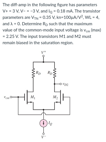
Transcribed Image Text:The diff-amp in the following figure has parameters
V+3 V, V = -3 V, and IQ = 0.18 mA. The transistor
parameters are VTN = 0.35 V, kn=100μA/V2, WL = 4,
and = 0. Determine RD such that the maximum
value of the common-mode input voltage is Vcm (max)
= 2.25 V. The input transistors M1 and M2 must
remain biased in the saturation region.
V+
ww
Rp
ww
RD
VD2
Vcm
M1
M2
Expert Solution
Check MarkThis question has been solved!
Explore an expertly crafted, step-by-step solution for a thorough understanding of key concepts.
bartleby
Step by stepSolved in 2 steps with 3 images
Knowledge Booster
Background pattern image
Similar questions
- circuits by using the small signal models of the transistor. Assume the Early voltage of the transistors are infinitely large. Calculate the small-signal input and output impedances of the following Vcc R1 R1 Rout VB RE Rin R2arrow_forwardThe n-channel JFET and the D-MOSFET have very similar I-V output characteristics. Which of these two structures can be operated in enhancement mode and why is that possible.arrow_forward........ (Figure-1) R. RB= 380kN,Rc= 1kN B = 100, VBB = Vcc=12V RB ww Vec CC ......... I, V CE СЕ V ВЕ BB Q-1-b) Describe briefly the input / output characteristics and application of Common Emitter BJT Configurationarrow_forward
- 4) Consider the clamping circuit below, assume Vref=3 V and Vin=5sin(wt) ..Draw the output voltage waveform. Clearly mark the max and min of the voltage.. Vrefarrow_forwardThe transistor parameters for the circuit in Figure are B, =B2 = 100, VBE1on) = VBE2ton) = 0.7 V, and %3D VA1 =VA2 =0.Find the small signal voltage gain Av = vo/vs. (Note that V-=0.026 V) Vcc=9 V Rib Q1 Vs 1 ko -Ro 20 V 100 Q -wwarrow_forwardThe DC Current Gain of a Transistor is Select one: a. Ratio of Collector Current to Base Current b. Ratio of Base Current to Collector Current c. Ratio of Emitter Current to Collector Current d. Ratio of Base Current to Emitter Currentarrow_forward
- II.The following figure shows a class AB amplifier. (a) Determine the parameters of dc VB (Q1), VB (Q2), VE, ICQ, VCEQ (Q1), VCEQ (Q2). (b) For a 5-Vrms input, determine the power that is provided to the load resistor, and (c) Draw the output signal +Vcc +9 V 1.0kn D: R 5.0 V rms R2 10 kN -Vecarrow_forwardA single stage amplifoer has a single stage of 60. The collector load of 500 ohms and the input impedance is 1kilo ohms. Calculate the overall gain when two such stages are cascaded through R-C coupling.arrow_forwardPlease solve with work shown. Will upvotearrow_forward
- 1. A certain phototransistor has a BDC. 150. If I = 250, what is the collector current? 2. In the figure below, if Vcc is replaced from a 12-V to an 18-V source. what would be output voltage when (a) the light source is OFF and (b) when the light source is ON. #12 Varrow_forwardwhich of the following configurations has low impedance and high output impedance? a. common-base. c. common-collector. b. common-emitter. d. all of these.arrow_forwardDetermine VB, VE, VC, VCE, IB, IE, and IC in Figure. The 2N3904 is a general purpose transistor with a typical BDC 200 Vcc +30 V WWII VCE VB R1 • 22 ΚΩ IC(mA) Chọn... * Chọn... * IB(UA) Chọn... * IE(MA) Chọn... ◆だいやまーく Chọn... * Chọn... * Chọn... * VE VC R2 ́ 10 ΚΩ www Rc 1.0 ΚΩ 2N3904 PDC=200 RE 1.0 ΚΩarrow_forward
arrow_back_ios
SEE MORE QUESTIONS
arrow_forward_ios
Recommended textbooks for you
- Text book imagePower System Analysis and Design (MindTap Course ...Electrical EngineeringISBN:9781305632134Author:J. Duncan Glover, Thomas Overbye, Mulukutla S. SarmaPublisher:Cengage Learning
Text book image
Power System Analysis and Design (MindTap Course ...
Electrical Engineering
ISBN:9781305632134
Author:J. Duncan Glover, Thomas Overbye, Mulukutla S. Sarma
Publisher:Cengage Learning