

A standalone scripting engine for KiCad footprints and PCBs.
- Implement MVP
- Generation of Kicad Modules (footprints)
- Ability to specify custom parameters, so script behaviour can be customized
- Loading of existing modules so they can be edited / combined
- Implement generation of text using custom fonts
- Generate / edit KiCad PCBs
Make sure you have Go 1.13+ installed.
go get github.com/twitchyliquid64/kcgen
go build -o kcgen github.com/twitchyliquid64/kcgen/kcgen
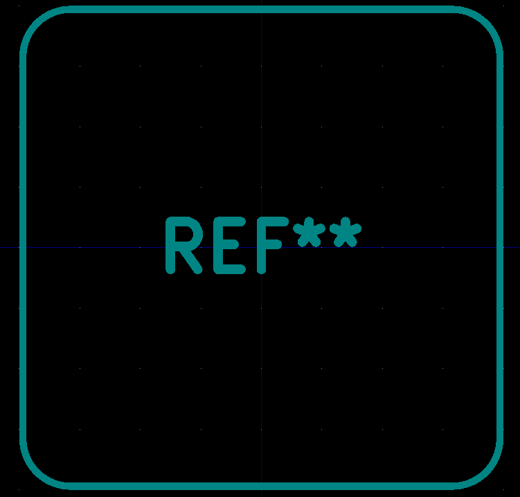
# You should now have the binary kcgen in your current directory.Make a file rounded_box.kcsl
load("mod.lib", m="graphics", p="pads")
load("shapes.lib", "shapes")
load("draw.lib", "draw")
mod = Mod(
 name = "test",
 layer = layers.front.copper,
 description = "This is a test module to demonstrate module generation.",
 attrs = ["virtual"],
 graphics = [m.ref()] +
 draw.mod.outline(shapes.box(10, 10, rounded_radius=1)),
)
Execute the script like this: ./kcgen -o rounded_box.kicad_mod rounded_box.kcsl
This example demonstrates some more advanced concepts, like using variables, expressions, and list comprehensions to compute equations and loop multiple times.
Execute the script like this: ./kcgen -o soic.kicad_mod soic.kcsl
load("mod.lib", m="graphics", p="pads")
load("shapes.lib", "shapes")
load("draw.lib", "draw")
# Configurable parameters.
pad_size = XY(x=1.95, y=0.6)
dist_between_rows = 4.95
pitch = 1.27
pins = 8
extra_clearance = XY(0.5, 0.3)
width = dist_between_rows + pad_size.x
height = pins * pitch / 2
first_pad_y = -(height/2 - pitch/2)
mod = Mod(
 name = "SOIC-8_" + str(width) + "x" + str(height) + "_" + str(pitch),
 layer = layers.front.copper,
 description = "An 8 pin SOIC footprint.",
 tags = ["soic", "smd"],
 attrs = ["smd"],
 graphics = [m.ref(XYZ(0, 0))] +
 draw.mod.outline(shapes.box(width + extra_clearance.x,
 height + extra_clearance.y),
 layer=layers.front.courtyard),
 pads = [ # left row
 p.smd(str(x+1),
 center = XY(-1 * dist_between_rows / 2, first_pad_y + x*pitch),
 size = pad_size,
 ) for x in range(int(pins/2))
 ] + [ # right row
 p.smd(str(x+1+int(pins/2)),
 center = XY(dist_between_rows / 2, first_pad_y + x*pitch),
 size = pad_size,
 ) for x in range(int(pins/2))
 ],
)
You can find more scripts in kcgen/example
| Function | Description | Example |
|---|---|---|
load |
Imports identifiers from a helper library or another script relative to the current directory. | load("draw.lib", "draw") - Imports the 'draw' symbol from the draw helper library. |
print |
Writes the argument to standard output. | print("Hello world") - Prints Hello world. |
range |
Generates a list of numbers based on the arguments provided. Identical to python. | range(3) generates [0, 1, 2]. |
XY |
Specifies coordinates in 2D. | XY(1,2) - coordinates are x=1 and y=2.XY(x=3, y=4) - coordinates are x=3 and y=4. |
XYZ |
Specifies coordinates in 3D. | XY(1,2,3) - coordinates are x=1, y=2, and z=3.XYZ(x=3) - coordinates are x=3, y=0, and z=0. |
Mod |
Generates a KiCad Module with the specified parameters. | See examples in previous section. |
TextPoly |
Generates a list of module polygons that represent text rendered with the provided font. | See textpoly.kcsl example. |
text.load_mod |
Loads a module from a file in the filesystem. | See composite.kcsl example. |
For a full list of Starlark constructs and builtin functions, please refer to the Starlark language spec.
| Constant | ||
|---|---|---|
layers |
Gives easy access to all the layer names, and the set of layer names typically used for smd & th pads. | layers.front.copper layers.front.fab layers.front.silkscreen layers.front.courtyard layers.front.paste layers.back... layers.smd layers.th layers.edge |
shape |
Different kinds of pad shapes. | shape.rect shape.circle shape.oval shape.round_rect |
defaults |
Typical values used as a default by KiCad | defaults.width defaults.thickness defaults.clearance |
pad |
Different kinds of pad. | pad.through_hole pad.np_through_hole pad.smd |
text |
Different kinds of module text element. | text.reference text.user text.value text.vertical |
zone_connect |
The modes controlling how a pad should connect to an adjacent zone of the same net. | zone_connect.inherited zone_connect.none zone_connect.thermal |
In addition to native functions available in your scripts, there are a number of helper libraries to help accomplish common tasks and make simple tasks shorter.
mod.lib has shorthands for generating pads & graphical elements for modules. Import either the graphics or pads identifier (or both), like this:
load("mod.lib", m="graphics")
# You can now call graphics functions like m.blah.
| Function | Description | Example |
|---|---|---|
graphics.ref() |
Places a text label that describes the reference (designator) of the module. | graphics.ref() - Place reference at XY(0,0).graphics.ref(XYZ(2,2)) - Place reference at XY(2,2).graphics.ref(XYZ(2,2, text.vertical)) - Place vertical reference at XY(2,2). |
graphics.text() |
Places a text element. | graphics.text(pos=XYZ(1,2), content='a') - Add a text element at XY(1,2) that says A. |
graphics.line() |
Places a line. You can also specify layer and width attributes. |
graphics.line(start=XY(), end=XY(2,2)) - Add a line from XY(0,0) to XY(2,2). |
graphics.circle() |
Draws the outline of a circle. | TODO |
graphics.poly() |
Draws a filled-in polygon using the specified points. | TODO |
graphics.arc() |
Draws an arc. | m.arc(center=XY(), end=XY(5), angle=45.0) |
graphics.filter() |
Filters out graphical with a certain type from a list of graphical elements. | m.filter(graphics_list, filter="fp_text") - Gets rid of all text graphics from graphics_list, returning a new list. |
load("mod.lib", "pads")
# You can now call pad functions like p.blah.
| Function | Description | Example |
|---|---|---|
pads.th() |
Generates a through-hole pad. | pads.th("2", center = XY(4, 3)) - Generates a pad called 2 at XY(4,3). The drill defaults to XY(1,1) and pad size to XY(1.7,1.7). |
pads.smd() |
Generates a surface-mount pad. | p.smd("1", center = XY(1,3)) - Creates a smd pad at XY(1,3).The size defaults to XY(1.4, 1.8) and the shape to a rectangle. |
pcb.lib has shorthands for generating elements for PCBs.
load("pcb.lib", p="pcb")
| Function | Description | Example |
|---|---|---|
p.line() |
Places a line. You can also specify layer and width attributes. |
pcb.line(start=XY(), end=XY(2,2)) - Add a line from XY(0,0) to XY(2,2). |
p.arc() |
Draws an arc. You can also specify layer and width attributes. |
pcb.arc(center=XY(), end=XY(5), angle=45.0, layer = layer.edge) |
p.text() |
Draws text on the PCB. | |
p.via() |
Places a via on the PCB. | |
p.track() |
Draws a track on the PCB. |
draw.lib has drawing shorthands.
load("draw.lib", "draw")
| Function | Description | Example |
|---|---|---|
draw.mod.outline() |
Returns the set of lines which fully connect the given points. You can also specify layer and width attributes. |
|
draw.pcb.outline() |
Returns the set of lines which fully connect the given points. You can also specify layer and width attributes. |
load("flatten.lib", "flatten")
| Function | Description | Example |
|---|---|---|
flatten.pads() |
Returns a list of equivalently placed graphics on the Fab layer, for the given list of pads. | flatten.pads(button.pads) |
flatten.graphics() |
Returns a list of equivalently placed graphics on the Fab layer, for the given list of graphics. | flatten.graphics(button.graphics) |
load("math.lib", "math")
# You can now call math functions like math.blah.
| Function | Description | Example |
|---|---|---|
math.point_on_circle() |
Computes the point radius distance from center, at the angle denoted by angle in radians. |
TODO |
math.point_on_circle_degrees() |
Computes the point radius distance from center, at the angle denoted by angle in degrees. |
TODO |
math.point_arc() |
Computes the set of points which interpolate an arc from start_angle to end_angle (radians) around center, with a radius denoted by radius. |
TODO |
math.x_array_within() |
Computes num_cols number of XY positions between width, centered at offset. |
TODO |