From working with classical microcontrollers, I am used to the fact that pins in input mode appear to have high input impedance - when connecting them to a high voltage, only a small current flows, and the voltage is sampled in order to obtain a digital state reading.
I'm using a ice40-HX8K FPGA, and I have a pin set to input, and connected to some inner working of my core. When I briefly connect the voltage supply to the pin, it is indeed registered as a digital HIGH by my core (it's an interrupt line), but such a high current flows that the whole board browns out for a split second.
The external circuit looks as following:
enter image description here
The pin is declared as an input in my top level module:
module top(
 // ...
 input INT0
)
And connected to a pin of the FPGA in my pin constraint file:
set_io INT0 P16
Did I understand something wrong here? Are FPGA input pins low impedance?
-
1\$\begingroup\$ Please add schematics what you are connecting and how, and what voltages are involved. \$\endgroup\$Justme– Justme2020年03月02日 22:58:52 +00:00Commented Mar 2, 2020 at 22:58
-
\$\begingroup\$ @Justme I added the circuit diagram. \$\endgroup\$Katharina– Katharina2020年03月02日 23:03:49 +00:00Commented Mar 2, 2020 at 23:03
-
\$\begingroup\$ What is the power supply voltage for the IO bank that P16 is part of? \$\endgroup\$The Photon– The Photon2020年03月02日 23:08:54 +00:00Commented Mar 2, 2020 at 23:08
-
\$\begingroup\$ @ThePhoton I assume it is 3.3V, because all testpoints on the board show 3.3V and connecting 1.2V is registered as a logical LOW. But I sadly have no idea how to specify that in the PCF. \$\endgroup\$Katharina– Katharina2020年03月02日 23:11:08 +00:00Commented Mar 2, 2020 at 23:11
-
\$\begingroup\$ For some reason, one of the I/O banks of my board does in fact use 1.2V as the supply voltage, which of course is asking for trouble when using a 3.3V signal to drive the pins. Switching to a 3.3V bank solved the problem. I am wondering though why the 1.2V supply voltage wasn't high enough to trigger a digital high then? (Which was the reason why I tried 3.3V) \$\endgroup\$Katharina– Katharina2020年03月02日 23:19:56 +00:00Commented Mar 2, 2020 at 23:19
1 Answer 1
Based on the comments it seems you were trying to drive a 1.2V IO bank from a 3.3V input.
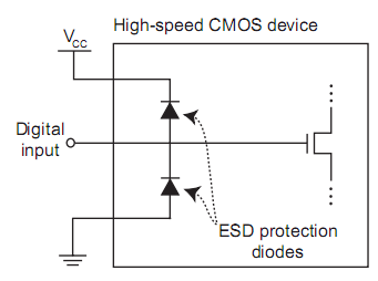
In many devices, CMOS inputs are protected using clamp diodes to reduce the risk of damage by ESD strikes. These diodes are shown in the picture below - connecting from the input to VCC, and from GND to the input.
For a 1.2V IO bank, the VCC will be 1.2V. If you connect the input directly to a 3.3V supply, you will forward bias this protection diode causing a very large current flow, most likely frying the diode protection in the process.
In your case the current flow was enough to brown out the supply.
There are ways of adding some protection for such occurances. However the best solution is to always ensure your input voltages match the IO bank specifications for your circuit.
One is to add a series resistor between the IO pin and your input circuit, this would help limit the current flow through the diode - the device datasheet should give a maximum current flow through the protection diodes.
The second is to swap your button around such that the pull-up resistor goes to the supply rail (limits current to a low level), and the button goes to ground. However even in this case you ought to check the datasheet to make sure that the diodes are rated for the resulting over-voltage on the input pins.
Explore related questions
See similar questions with these tags.