I'm trying to get a Bluefruit Feather M0, which has a SAMD21G on it, to do high-frequency PWM by accessing timer registers directly, rather than using the Arduino API to do PWM at ~1 kHz or ~500 Hz. Actual frequency isn't important at this stage, I just want a lot more than 1 kHz.
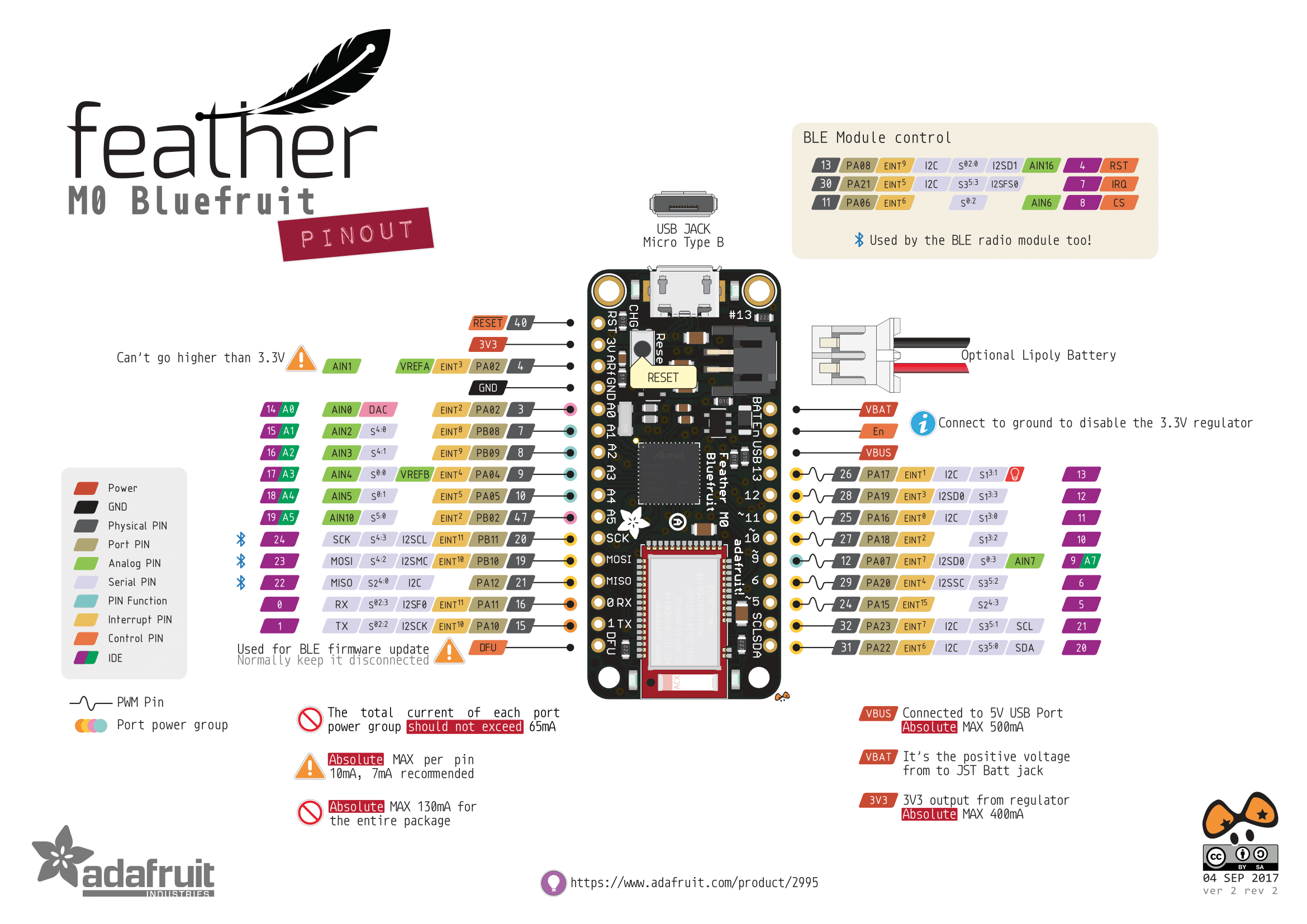
I found an example for an MKR1000, based on a similar processor. I've adapted it as shown below. Comparing the Adafruit pinout with the original code and with the datasheet, it's apparent that the pin numberings are different and that pin 11, which is the only one of the two example pins that is accessible, is on TCC0 here and not TCC1.
The only change I see that I needed to make is to duplicate all the TCC1 setup in setupTimers() and the TCC1 duty cycle control in loop() for TCC0. Yet on the scope, I see no PWM output. I then tried setting pin 13 to PWM as well, so I'd see it on the on board LED. Still nothing. I'm somewhat stuck now.
Does anyone have any ideas?
void setup() {
 // put your setup code here, to run once:
 setupTimers();
 Serial.begin(9600);
}
void loop() {
 // put your main code here, to run repeatedly:
 int t = 0;
 Serial.println("\nRunning PWM 0 to 100%");
 for (t = 0; t < 1000; t = t + 1) {
 REG_TCC1_CC1 = t; // TCC1 CC1 - on D3 - PWM signalling
 while (TCC1->SYNCBUSY.bit.CC1); // Wait for synchronization
 REG_TCC0_CC1 = t; // TCC1 CC1 - on D3 - PWM signalling
 while (TCC0->SYNCBUSY.bit.CC1); // Wait for synchronization
 delay(1);
 Serial.print(".");
 }
 delay(2000);
}
// Output PWM 24Khz on digital pin D3 and D11 using timer TCC1 (10-bit resolution)
void setupTimers() {
 REG_GCLK_GENDIV = GCLK_GENDIV_DIV(1) | // Divide the 48MHz clock source by divisor N=1: 48MHz/1=48MHz
 GCLK_GENDIV_ID(4); // Select Generic Clock (GCLK) 4
 while (GCLK->STATUS.bit.SYNCBUSY); // Wait for synchronization
 REG_GCLK_GENCTRL = GCLK_GENCTRL_IDC | // Set the duty cycle to 50/50 HIGH/LOW
 GCLK_GENCTRL_GENEN | // Enable GCLK4
 GCLK_GENCTRL_SRC_DFLL48M | // Set the 48MHz clock source
 GCLK_GENCTRL_ID(4); // Select GCLK4
 while (GCLK->STATUS.bit.SYNCBUSY); // Wait for synchronization
 // Enable the port multiplexer for the digital pin D3 and D11 **** g_APinDescription() converts Arduino Pin to SAMD21 pin
 PORT->Group[g_APinDescription[3].ulPort].PINCFG[g_APinDescription[3].ulPin].bit.PMUXEN = 1;
 PORT->Group[g_APinDescription[11].ulPort].PINCFG[g_APinDescription[11].ulPin].bit.PMUXEN = 1;
 PORT->Group[g_APinDescription[13].ulPort].PINCFG[g_APinDescription[13].ulPin].bit.PMUXEN = 1;
 // Connect the TCC1 timer to digital output D3 and D11 - port pins are paired odd PMUO and even PMUXE
 // F & E specify the timers: TCC0, TCC1 and TCC2
 PORT->Group[g_APinDescription[2].ulPort].PMUX[g_APinDescription[2].ulPin >> 1].reg = PORT_PMUX_PMUXO_E; // D3 is on PA11 = odd, use Device E on TCC1/WO[1]
 PORT->Group[g_APinDescription[11].ulPort].PMUX[g_APinDescription[11].ulPin >> 1].reg = PORT_PMUX_PMUXE_F; // D11 is on PA08 = even, use device F on TCC1/WO[0]
 PORT->Group[g_APinDescription[13].ulPort].PMUX[g_APinDescription[13].ulPin >> 1].reg = PORT_PMUX_PMUXE_E; // Try the LED.. doesn't work with E or F
 //Actually, pin 11 on the Feather is on PA16. Still even, not sure of the significance, but it's now TCC0/WO[6] and still port F.
 //All the stuff further down is about TCC1!
 // Feed GCLK4 to TCC0 and TCC1
 REG_GCLK_CLKCTRL = GCLK_CLKCTRL_CLKEN | // Enable GCLK4 to TCC0 and TCC1
 GCLK_CLKCTRL_GEN_GCLK4 | // Select GCLK4
 GCLK_CLKCTRL_ID_TCC0_TCC1; // Feed GCLK4 to TCC0 and TCC1
 while (GCLK->STATUS.bit.SYNCBUSY); // Wait for synchronization
 // Dual slope PWM operation: timers countinuously count up to PER register value then down 0
 REG_TCC1_WAVE |= TCC_WAVE_POL(0xF) | // Reverse the output polarity on all TCC0 outputs
 TCC_WAVE_WAVEGEN_DSBOTH; // Setup dual slope PWM on TCC0
 while (TCC1->SYNCBUSY.bit.WAVE); // Wait for synchronization
 // Each timer counts up to a maximum or TOP value set by the PER register,
 // this determines the frequency of the PWM operation: Freq = 48Mhz/(2*N*PER)
 REG_TCC1_PER = 1000; // Set the FreqTcc of the PWM on TCC1 to 24Khz
 while (TCC1->SYNCBUSY.bit.PER); // Wait for synchronization
 // Set the PWM signal to output , PWM ds = 2*N(TOP-CCx)/Freqtcc => PWM=0 => CCx=PER, PWM=50% => CCx = PER/2
 REG_TCC1_CC1 = 500; // TCC1 CC1 - on D3 50%
 while (TCC1->SYNCBUSY.bit.CC1); // Wait for synchronization
 REG_TCC1_CC0 = 500; // TCC1 CC0 - on D11 50%
 while (TCC1->SYNCBUSY.bit.CC0); // Wait for synchronization
 // Divide the GCLOCK signal by 1 giving in this case 48MHz (20.83ns) TCC1 timer tick and enable the outputs
 REG_TCC1_CTRLA |= TCC_CTRLA_PRESCALER_DIV1 | // Divide GCLK4 by 1
 TCC_CTRLA_ENABLE; // Enable the TCC0 output
 while (TCC1->SYNCBUSY.bit.ENABLE); // Wait for synchronization
 //Do everything again for TCC0
 // Dual slope PWM operation: timers countinuously count up to PER register value then down 0
 REG_TCC0_WAVE |= TCC_WAVE_POL(0xF) | // Reverse the output polarity on all TCC0 outputs
 TCC_WAVE_WAVEGEN_DSBOTH; // Setup dual slope PWM on TCC0
 while (TCC0->SYNCBUSY.bit.WAVE); // Wait for synchronization
 // Each timer counts up to a maximum or TOP value set by the PER register,
 // this determines the frequency of the PWM operation: Freq = 48Mhz/(2*N*PER)
 REG_TCC0_PER = 1000; // Set the FreqTcc of the PWM on TCC1 to 24Khz
 while (TCC0->SYNCBUSY.bit.PER); // Wait for synchronization
 // Set the PWM signal to output , PWM ds = 2*N(TOP-CCx)/Freqtcc => PWM=0 => CCx=PER, PWM=50% => CCx = PER/2
 REG_TCC0_CC1 = 500; // TCC1 CC1 - on D3 50%
 while (TCC0->SYNCBUSY.bit.CC1); // Wait for synchronization
 REG_TCC0_CC0 = 500; // TCC1 CC0 - on D11 50%
 while (TCC0->SYNCBUSY.bit.CC0); // Wait for synchronization
 // Divide the GCLOCK signal by 1 giving in this case 48MHz (20.83ns) TCC1 timer tick and enable the outputs
 REG_TCC0_CTRLA |= TCC_CTRLA_PRESCALER_DIV1 | // Divide GCLK4 by 1
 TCC_CTRLA_ENABLE; // Enable the TCC0 output
 while (TCC0->SYNCBUSY.bit.ENABLE); // Wait for synchronization
}
-
If you only want a PWM signal on D11 (PA16 on your MCU) then do not configure other pins from which you you know they are not supported. Perhaps your program crashes. Do you see the "." on the serial monitor? BTW: the example does configure D2 instead of D3 by accident. But now you need only D11 ;-). Then do not configure both TCC, just the one you need.Peter Paul Kiefer– Peter Paul Kiefer2019年12月18日 18:09:33 +00:00Commented Dec 18, 2019 at 18:09
1 Answer 1
For your specific problem: the Feather's D11 is the SAMD's PA16 and on TCC0/WO[6] (use REG_TCC0_CCB2 and PORT_PMUX_PMUXE_F), and also on TCC2/WO[0] (use REG_TCC2_CCB0 and PORT_PMUX_PMUXE_E).
An easier way: I have made a high-frequency-PWM library for this (called Arduino_SAMD21_turbo_PWM), and I have implemented the pin table for the Adafruit Feather M0.
I haven't tested it though, mainly because I don't have an Adafruit Feather M0. Still, feel free to have a try.
The pin mapping table itself for the Adafruit Feather M0, which AFAIK has the same pin mappings as the Arduino Zero, is here on Github; maybe it can help as well.
Explore related questions
See similar questions with these tags.