Tensor Processing Unit
| Tensor Processing Unit 3.0 | |
| Designer | |
|---|---|
| Introduced | 2015[1] |
| Type | Neural network Machine learning |
Tensor Processing Unit (TPU) is an AI accelerator application-specific integrated circuit (ASIC) developed by Google for neural network machine learning, using Google's own TensorFlow software.[2] Google began using TPUs internally in 2015, and in 2018 made them available for third-party use, both as part of its cloud infrastructure and by offering a smaller version of the chip for sale.
Comparison to CPUs and GPUs
[edit ]Compared to a graphics processing unit, TPUs are designed for a high volume of low precision computation (e.g. as little as 8-bit precision)[3] with more input/output operations per joule, without hardware for rasterisation/texture mapping.[4] The TPU ASICs are mounted in a heatsink assembly, which can fit in a hard drive slot within a data center rack, according to Norman Jouppi.[5]
Different types of processors are suited for different types of machine learning models. TPUs are well suited for CNNs, while GPUs have benefits for some fully-connected neural networks, and CPUs can have advantages for RNNs.[6]
History
[edit ]According to Jonathan Ross, one of the original TPU engineers,[1] and later the founder of Groq, three separate groups at Google were developing AI accelerators, with the TPU being the design that was ultimately selected. He was not aware of systolic arrays at the time and upon learning the term thought "Oh, that's called a systolic array? It just seemed to make sense."[7]
The tensor processing unit was announced in May 2016 at Google I/O, when the company said that the TPU had already been used inside their data centers for over a year.[5] [4] Google's 2017 paper describing its creation cites previous systolic matrix multipliers of similar architecture built in the 1990s.[8] The chip has been specifically designed for Google's TensorFlow framework, a symbolic math library which is used for machine learning applications such as neural networks.[9] However, as of 2017 Google still used CPUs and GPUs for other types of machine learning.[5] Other AI accelerator designs are appearing from other vendors also and are aimed at embedded and robotics markets.
Google's TPUs are proprietary. Some models are commercially available, and on February 12, 2018, The New York Times reported that Google "would allow other companies to buy access to those chips through its cloud-computing service."[10] Google has said that they were used in the AlphaGo versus Lee Sedol series of human-versus-machine Go games,[4] as well as in the AlphaZero system, which produced Chess, Shogi and Go playing programs from the game rules alone and went on to beat the leading programs in those games.[11] Google has also used TPUs for Google Street View text processing and was able to find all the text in the Street View database in less than five days. In Google Photos, an individual TPU can process over 100 million photos a day.[5] It is also used in RankBrain which Google uses to provide search results.[12]
Google provides third parties access to TPUs through its Cloud TPU service as part of the Google Cloud Platform [13] and through its notebook-based services Kaggle and Colaboratory.[14] [15]
Products
[edit ]| TPUv1 | TPUv2 | TPUv3 | TPUv4[17] [19] [20] | TPUv5e[21] | TPUv5p[22] [23] | v6e (Trillium)[24] [25] | |
|---|---|---|---|---|---|---|---|
| Date introduced | 2015 | 2017 | 2018 | 2021 | 2023 | 2023 | 2024 |
| Process node | 28 nm | 16 nm | 16 nm | 7 nm | Unstated | Unstated | |
| Die size (mm2) | 331 | < 625 | < 700 | < 400 | 300-350 | Unstated | |
| On-chip memory (MiB) | 28 | 32 | 32 (VMEM) + 5 (spMEM) | 128 (CMEM) + 32 (VMEM) + 10 (spMEM) | 48[citation needed ] | 112[citation needed ] | |
| Clock speed (MHz) | 700 | 700 | 940 | 1050 | Unstated | 1750 | |
| Memory | 8 GiB DDR3 | 16 GiB HBM | 32 GiB HBM | 32 GiB HBM | 16 GB HBM | 95 GB HBM | 32 GB |
| Memory bandwidth | 34 GB/s | 600 GB/s | 900 GB/s | 1200 GB/s | 819 GB/s | 2765 GB/s | 1640 GB/s |
| TDP (W) | 75 | 280 | 220 | 170 | Not Listed | Not Listed | |
| TOPS (Tera Operations Per Second) | 23 | 45 | 123 | 275 | 197 (bf16)
393 (int8) |
459 (bf16)
918 (int8) |
918 (bf16)
1836 (int8) |
| TOPS/W | 0.31 | 0.16 | 0.56 | 1.62 | Not Listed | Not Listed |
First generation TPU
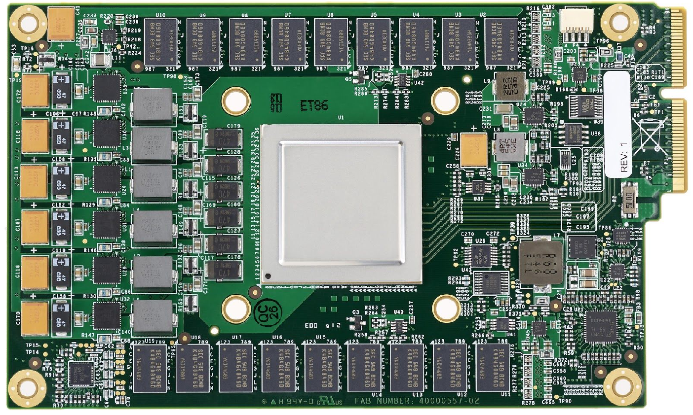
[edit ]The first-generation TPU is an 8-bit matrix multiplication engine, driven with CISC instructions by the host processor across a PCIe 3.0 bus. It is manufactured on a 28 nm process with a die size ≤ 331 mm 2. The clock speed is 700 MHz and it has a thermal design power of 28–40 W. It has 28 MiB of on chip memory, and 4 MiB of 32-bit accumulators taking the results of a ×ばつ256 systolic array of 8-bit multipliers.[8] Within the TPU package is 8 GiB of dual-channel 2133 MHz DDR3 SDRAM offering 34 GB/s of bandwidth.[18] Instructions transfer data to or from the host, perform matrix multiplications or convolutions, and apply activation functions.[8]
Second generation TPU
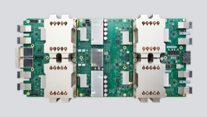
[edit ]The second-generation TPU was announced in May 2017.[26] Google stated the first-generation TPU design was limited by memory bandwidth and using 16 GB of High Bandwidth Memory in the second-generation design increased bandwidth to 600 GB/s and performance to 45 teraFLOPS.[18] The TPUs are then arranged into four-chip modules with a performance of 180 teraFLOPS.[26] Then 64 of these modules are assembled into 256-chip pods with 11.5 petaFLOPS of performance.[26] Notably, while the first-generation TPUs were limited to integers, the second-generation TPUs can also calculate in floating point, introducing the bfloat16 format invented by Google Brain. This makes the second-generation TPUs useful for both training and inference of machine learning models. Google has stated these second-generation TPUs will be available on the Google Compute Engine for use in TensorFlow applications.[27]
Third generation TPU
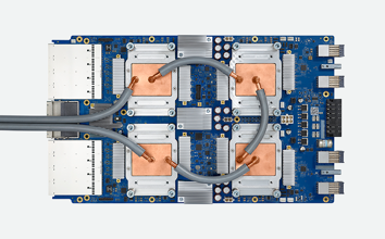
[edit ]The third-generation TPU was announced on May 8, 2018.[28] Google announced that processors themselves are twice as powerful as the second-generation TPUs, and would be deployed in pods with four times as many chips as the preceding generation.[29] [30] This results in an 8-fold increase in performance per pod (with up to 1,024 chips per pod) compared to the second-generation TPU deployment.
Fourth generation TPU
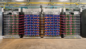
[edit ]On May 18, 2021, Google CEO Sundar Pichai spoke about TPU v4 Tensor Processing Units during his keynote at the Google I/O virtual conference. TPU v4 improved performance by more than 2x over TPU v3 chips. Pichai said "A single v4 pod contains 4,096 v4 chips, and each pod has 10x the interconnect bandwidth per chip at scale, compared to any other networking technology."[31] An April 2023 paper by Google claims TPU v4 is 5-87% faster than an Nvidia A100 at machine learning benchmarks.[32]
There is also an "inference" version, called v4i,[33] that does not require liquid cooling.[34]
Fifth generation TPU
[edit ]In 2021, Google revealed the physical layout of TPU v5 is being designed with the assistance of a novel application of deep reinforcement learning.[35] Google claims TPU v5 is nearly twice as fast as TPU v4,[36] and based on that and the relative performance of TPU v4 over A100, some speculate TPU v5 as being as fast as or faster than an H100.[37]
Similar to the v4i being a lighter-weight version of the v4, the fifth generation has a "cost-efficient"[38] version called v5e.[21] In December 2023, Google announced TPU v5p which is claimed to be competitive with the H100.[39]
Sixth generation TPU
[edit ]In May 2024, at the Google I/O conference, Google announced TPU v6, which became available in preview in October 2024.[40] Google claimed a 4.7 times performance increase relative to TPU v5e,[41] via larger matrix multiplication units and an increased clock speed. High bandwidth memory (HBM) capacity and bandwidth have also doubled. A pod can contain up to 256 Trillium units.[42]
Edge TPU
[edit ]In July 2018, Google announced the Edge TPU. The Edge TPU is Google's purpose-built ASIC chip designed to run machine learning (ML) models for edge computing, meaning it is much smaller and consumes far less power compared to the TPUs hosted in Google datacenters (also known as Cloud TPUs[43] ). In January 2019, Google made the Edge TPU available to developers with a line of products under the Coral brand. The Edge TPU is capable of 4 trillion operations per second with 2 W of electrical power.[44]
The product offerings include a single-board computer (SBC), a system on module (SoM), a USB accessory, a mini PCI-e card, and an M.2 card. The SBC Coral Dev Board and Coral SoM both run Mendel Linux OS – a derivative of Debian.[45] [46] The USB, PCI-e, and M.2 products function as add-ons to existing computer systems, and support Debian-based Linux systems on x86-64 and ARM64 hosts (including Raspberry Pi).
The machine learning runtime used to execute models on the Edge TPU is based on TensorFlow Lite.[47] The Edge TPU is only capable of accelerating forward-pass operations, which means it's primarily useful for performing inferences (although it is possible to perform lightweight transfer learning on the Edge TPU[48] ). The Edge TPU also only supports 8-bit math, meaning that for a network to be compatible with the Edge TPU, it needs to either be trained using the TensorFlow quantization-aware training technique, or since late 2019 it's also possible to use post-training quantization.
On November 12, 2019, Asus announced a pair of single-board computer (SBCs) featuring the Edge TPU. The Asus Tinker Edge T and Tinker Edge R Board designed for IoT and edge AI. The SBCs officially support Android and Debian operating systems.[49] [50] ASUS has also demonstrated a mini PC called Asus PN60T featuring the Edge TPU.[51]
On January 2, 2020, Google announced the Coral Accelerator Module and Coral Dev Board Mini, to be demonstrated at CES 2020 later the same month. The Coral Accelerator Module is a multi-chip module featuring the Edge TPU, PCIe and USB interfaces for easier integration. The Coral Dev Board Mini is a smaller SBC featuring the Coral Accelerator Module and MediaTek 8167s SoC.[52] [53]
Pixel Neural Core
[edit ]On October 15, 2019, Google announced the Pixel 4 smartphone, which contains an Edge TPU called the Pixel Neural Core. Google describe it as "customized to meet the requirements of key camera features in Pixel 4", using a neural network search that sacrifices some accuracy in favor of minimizing latency and power use.[54]
Google Tensor
[edit ]Google followed the Pixel Neural Core by integrating an Edge TPU into a custom system-on-chip named Google Tensor, which was released in 2021 with the Pixel 6 line of smartphones.[55] The Google Tensor SoC demonstrated "extremely large performance advantages over the competition" in machine learning-focused benchmarks; although instantaneous power consumption also was relatively high, the improved performance meant less energy was consumed due to shorter periods requiring peak performance.[56]
Lawsuit
[edit ]In 2019, Singular Computing, founded in 2009 by Joseph Bates, a visiting professor at MIT,[57] filed suit against Google alleging patent infringement in TPU chips.[58] By 2020, Google had successfully lowered the number of claims the court would consider to just two: claim 53 of US 8407273 filed in 2012 and claim 7 of US 9218156 filed in 2013, both of which claim a dynamic range of 10−6 to 106 for floating point numbers, which the standard float16 cannot do (without resorting to subnormal numbers) as it only has five bits for the exponent. In a 2023 court filing, Singular Computing specifically called out Google's use of bfloat16, as that exceeds the dynamic range of float16.[59] Singular claims non-standard floating point formats were non-obvious in 2009, but Google retorts that the VFLOAT[60] format, with configurable number of exponent bits, existed as prior art in 2002.[61] By January 2024, subsequent lawsuits by Singular had brought the number of patents being litigated up to eight. Towards the end of the trial later that month, Google agreed to a settlement with undisclosed terms.[62] [63]
See also
[edit ]- Cognitive computer
- AI accelerator
- Structure tensor, a mathematical foundation for TPU's
- Tensor Core, a similar architecture by Nvidia
- TrueNorth, a similar device simulating spiking neurons instead of low-precision tensors
- Vision processing unit, a similar device specialised for vision processing
References
[edit ]- ^ a b Jouppi, Norman; et al. (2017). "In-Datacenter Performance Analysis of a Tensor Processing Unit". Proceedings of the 44th annual international symposium on computer architecture. International Symposium on Computer Architecture. Toronto: Association for Computing Machinery. pp. 1–12. arXiv:1704.04760 . doi:10.1145/3079856.3080246.
- ^ "Cloud Tensor Processing Units (TPUs)". Google Cloud. Retrieved 20 July 2020.
- ^ Armasu, Lucian (2016年05月19日). "Google's Big Chip Unveil For Machine Learning: Tensor Processing Unit With 10x Better Efficiency (Updated)". Tom's Hardware. Retrieved 2016年06月26日.
- ^ a b c Jouppi, Norm (May 18, 2016). "Google supercharges machine learning tasks with TPU custom chip". Google Cloud Platform Blog. Retrieved 2017年01月22日.
- ^ a b c d "Google's Tensor Processing Unit explained: this is what the future of computing looks like". TechRadar. Retrieved 2017年01月19日.
- ^ Wang, Yu Emma; Wei, Gu-Yeon; Brooks, David (2019年07月01日). "Benchmarking TPU, GPU, and CPU Platforms for Deep Learning". arXiv:1907.10701 [cs.LG].
- ^ Tensor Processing Unit on LinkedIn
- ^ a b c Jouppi, Norman P.; Young, Cliff; Patil, Nishant; Patterson, David; Agrawal, Gaurav; Bajwa, Raminder; Bates, Sarah; Bhatia, Suresh; Boden, Nan; Borchers, Al; Boyle, Rick; Cantin, Pierre-luc; Chao, Clifford; Clark, Chris; Coriell, Jeremy; Daley, Mike; Dau, Matt; Dean, Jeffrey; Gelb, Ben; Ghaemmaghami, Tara Vazir; Gottipati, Rajendra; Gulland, William; Hagmann, Robert; Ho, C. Richard; Hogberg, Doug; Hu, John; Hundt, Robert; Hurt, Dan; Ibarz, Julian; Jaffey, Aaron; Jaworski, Alek; Kaplan, Alexander; Khaitan, Harshit; Koch, Andy; Kumar, Naveen; Lacy, Steve; Laudon, James; Law, James; Le, Diemthu; Leary, Chris; Liu, Zhuyuan; Lucke, Kyle; Lundin, Alan; MacKean, Gordon; Maggiore, Adriana; Mahony, Maire; Miller, Kieran; Nagarajan, Rahul; Narayanaswami, Ravi; Ni, Ray; Nix, Kathy; Norrie, Thomas; Omernick, Mark; Penukonda, Narayana; Phelps, Andy; Ross, Jonathan; Ross, Matt; Salek, Amir; Samadiani, Emad; Severn, Chris; Sizikov, Gregory; Snelham, Matthew; Souter, Jed; Steinberg, Dan; Swing, Andy; Tan, Mercedes; Thorson, Gregory; Tian, Bo; Toma, Horia; Tuttle, Erick; Vasudevan, Vijay; Walter, Richard; Wang, Walter; Wilcox, Eric; Yoon, Doe Hyun (June 26, 2017). In-Datacenter Performance Analysis of a Tensor Processing UnitTM. Toronto, Canada. arXiv:1704.04760 .
- ^ "TensorFlow: Open source machine learning" "It is machine learning software being used for various kinds of perceptual and language understanding tasks" — Jeffrey Dean, minute 0:47 / 2:17 from Youtube clip
- ^ Metz, Cade (12 February 2018). "Google Makes Its Special A.I. Chips Available to Others". The New York Times. Retrieved 2018年02月12日.
- ^ McGourty, Colin (6 December 2017). "DeepMind's AlphaZero crushes chess". chess24.com.
- ^ "Google's Tensor Processing Unit could advance Moore's Law 7 years into the future". PCWorld. Retrieved 2017年01月19日.
- ^ "Frequently Asked Questions | Cloud TPU". Google Cloud. Retrieved 2021年01月14日.
- ^ "Google Colaboratory". colab.research.google.com. Retrieved 2021年05月15日.
- ^ "Use TPUs | TensorFlow Core". TensorFlow. Retrieved 2021年05月15日.
- ^ Jouppi, Norman P.; Yoon, Doe Hyun; Ashcraft, Matthew; Gottscho, Mark (June 14, 2021). Ten lessons from three generations that shaped Google's TPUv4i (PDF). International Symposium on Computer Architecture. Valencia, Spain. doi:10.1109/ISCA52012.2021.00010. ISBN 978-1-4503-9086-6.
- ^ a b "System Architecture | Cloud TPU". Google Cloud. Retrieved 2022年12月11日.
- ^ a b c Kennedy, Patrick (22 August 2017). "Case Study on the Google TPU and GDDR5 from Hot Chips 29". Serve The Home. Retrieved 23 August 2017.
- ^ Stay tuned, more information on TPU v4 is coming soon, retrieved 2020年08月06日.
- ^ "TPU v4: An Optically Reconfigurable Supercomputer for Machine Learning with Hardware Support for Embeddings".
- ^ a b Cloud TPU v5e Inference Public Preview, retrieved 2023年11月06日.
- ^ Cloud TPU v5p Google Cloud. retrieved 2024年04月09日
- ^ Cloud TPU v5p Training, retrieved 2024年04月09日.
- ^ "Introducing Trillium, sixth-generation TPUs". Google Cloud Blog. Retrieved 2024年05月29日.
- ^ "TPU v6e". Google Cloud. Retrieved 2024年11月10日.
- ^ a b c Bright, Peter (17 May 2017). "Google brings 45 teraflops tensor flow processors to its compute cloud". Ars Technica. Retrieved 30 May 2017.
- ^ Kennedy, Patrick (17 May 2017). "Google Cloud TPU Details Revealed". Serve The Home. Retrieved 30 May 2017.
- ^ Frumusanu, Andre (8 May 2018). "Google I/O Opening Keynote Live-Blog" . Retrieved 9 May 2018.
- ^ Feldman, Michael (11 May 2018). "Google Offers Glimpse of Third-Generation TPU Processor". Top 500. Retrieved 14 May 2018.
- ^ Teich, Paul (10 May 2018). "Tearing Apart Google's TPU 3.0 AI Coprocessor". The Next Platform. Retrieved 14 May 2018.
- ^ "Google Launches TPU v4 AI Chips". www.hpcwire.com. 20 May 2021. Retrieved June 7, 2021.
- ^ Jouppi, Norman (2023年04月20日). "TPU v4: An Optically Reconfigurable Supercomputer for Machine Learning with Hardware Support for Embeddings". arXiv:2304.01433 [cs.AR].
- ^ Kennedy, Patrick (2023年08月29日). "Google Details TPUv4 and its Crazy Optically Reconfigurable AI Network". servethehome.com. Retrieved 2023年12月16日.
- ^ "Why did Google develop its own TPU chip? In-depth disclosure of team members". censtry.com. 2021年10月20日. Retrieved 2023年12月16日.
- ^ Mirhoseini, Azalia; Goldie, Anna (2021年06月01日). "A graph placement methodology for fast chip design" (PDF). Nature . 594 (7962): 207–212. doi:10.1038/s41586-022-04657-6. PMID 35361999. S2CID 247855593 . Retrieved 2023年06月04日.
- ^ Vahdat, Amin (2023年12月06日). "Enabling next-generation AI workloads: Announcing TPU v5p and AI Hypercomputer" . Retrieved 2024年04月08日.
- ^ Afifi-Sabet, Keumars (2023年12月23日). "Google is rapidly turning into a formidable opponent to BFF Nvidia — the TPU v5p AI chip powering its hypercomputer is faster and has more memory and bandwidth than ever before, beating even the mighty H100". TechRadar . Retrieved 2024年04月08日.
- ^ "Expanding our AI-optimized infrastructure portfolio: Introducing Cloud TPU v5e and announcing A3 GA". 2023年08月29日. Retrieved 2023年12月16日.
- ^ "Enabling next-generation AI workloads: Announcing TPU v5p and AI Hypercomputer". 2023年12月06日. Retrieved 2024年04月09日.
- ^ Lohmeyer, Mark (2024年10月30日). "Powerful infrastructure innovations for your AI-first future".
- ^ Velasco, Alan (2024年05月15日). "Google Cloud Unveils Trillium, Its 6th-Gen TPU With A 4.7X AI Performance Leap". HotHardware . Retrieved 2024年05月15日.
- ^ "Introducing Trillium, sixth-generation TPUs". Google Cloud Blog. Retrieved 2024年05月17日.
- ^ "Cloud TPU". Google Cloud. Retrieved 2021年05月21日.
- ^ "Edge TPU performance benchmarks". Coral. Retrieved 2020年01月04日.
- ^ "Dev Board". Coral. Retrieved 2021年05月21日.
- ^ "System-on-Module (SoM)". Coral. Retrieved 2021年05月21日.
- ^ "Bringing intelligence to the edge with Cloud IoT". Google Blog. 2018年07月25日. Retrieved 2018年07月25日.
- ^ "Retrain an image classification model on-device". Coral. Retrieved 2019年05月03日.
- ^ "組込み総合技術展&IoT総合技術展「ET & IoT Technology 2019」に出展することを発表". Asus.com (in Japanese). Retrieved 2019年11月13日.
- ^ Shilov, Anton. "ASUS & Google Team Up for 'Tinker Board' AI-Focused Credit-Card Sized Computers". Anandtech.com. Retrieved 2019年11月13日.
- ^ Aufranc, Jean-Luc (2019年05月29日). "ASUS Tinker Edge T & CR1S-CM-A SBC to Feature Google Coral Edge TPU & NXP i.MX 8M Processor". CNX Software - Embedded Systems News. Retrieved 2019年11月14日.
- ^ "New Coral products for 2020". Google Developers Blog. Retrieved 2020年01月04日.
- ^ "Accelerator Module". Coral. Retrieved 2020年01月04日.
- ^ "Introducing the Next Generation of On-Device Vision Models: MobileNetV3 and MobileNetEdgeTPU". Google AI Blog. Retrieved 2020年04月16日.
- ^ Gupta, Suyog; White, Marie (November 8, 2021). "Improved On-Device ML on Pixel 6, with Neural Architecture Search". Google AI Blog. Retrieved 16 December 2022.
- ^ Frumusanu, Andrei (November 2, 2021). "Google's Tensor inside of Pixel 6, Pixel 6 Pro: A Look into Performance & Efficiency | Google's IP: Tensor TPU/NPU". AnandTech. Retrieved 16 December 2022.
- ^ Hardesty, Larry (2011年01月03日). "The surprising usefulness of sloppy arithmetic". MIT . Retrieved 2024年01月10日.
- ^ Bray, Hiawatha (2024年01月10日). "Local inventor challenges Google in billion-dollar patent fight". Boston Globe . Boston. Archived from the original on 2024年01月10日. Retrieved 2024年01月10日.
- ^ "SINGULAR COMPUTING LLC, Plaintiff, v. GOOGLE LLC, Defendant: Amended Complaint for Patent Infringement" (PDF). rpxcorp.com. RPX Corporation. 2020年03月20日. Retrieved 2024年01月10日.
- ^ Wang, Xiaojun; Leeser, Miriam (2010年09月01日). "VFloat: A Variable Precision Fixed- and Floating-Point Library for Reconfigurable Hardware". ACM Transactions on Reconfigurable Technology and Systems. 3 (3): 1–34. doi:10.1145/1839480.1839486 . Retrieved 2024年01月10日.
- ^ "Singular Computing LLC v. Google LLC". casetext.com. 2023年04月06日. Retrieved 2024年01月10日.
- ^ Calkins, Laurel Brubaker (January 24, 2024). "Google Settles AI-Chip Suit That Had Sought Over 5ドル Billion". Bloomberg Law.
- ^ Brittain, Blake; Raymond, Ray (January 24, 2024). "Google settles AI-related chip patent lawsuit that sought 1ドル.67 bln". Reuters.