Fundamentals of Analog/RF design: Noise, Signal, Power
Analog design does not scale the way digital design does. Namely, as process shrinks, one does not immediately benefit by having reduced power consumption for the same performance. I will show in this post the main constraint involved in analog/RF design: that to maintain a given SNR, a certain amount of power must be consumed by an analog/RF circuit.
Transconductors
MOS Thermal Noise
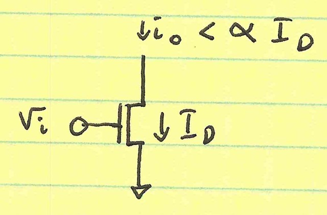
Shown below is a disembodied MOS transconductor:
It takes an input voltage vi and outputs a current io. To avoid clipping, io would need to be less than ID, the bias voltage on the MOS transistor. However, let’s say that for some linearity requirement (IM2, IM3, IM5, etc.) that we limit io to be less than ×ばつID.
So, we know the signal power is:
Psig = (×ばつID)2 = ×ばつID^2
This power is computed as a current; we could equally have the transconductor drive a specified load impedance and compute all the quantities as voltage, but they will not change the end result.
Likewise, the noise current power is:
Pnoise = ×ばつk×ばつgm×ばつB/3
At this point, it is useful to represent gm in terms of voltage and current:
gm = ×ばつID/VDSat
→ Pnoise = ×ばつk×ばつID×ばつB/(×ばつVDSat)
Therefore:
SNR = Psig/Pnoise = ×ばつID×ばつVDSat/(×ばつk×ばつB)
Note that the term ID×ばつVDSat is a lower-bound on the power dissipated across the FET. In fact, the actual power dissipated across the FET is ID×ばつVDS, which is actually greater than ID×ばつVDSat, since VDS > VDS to keep the FET in saturation.
To summarize:
- For a given SNR, we need a certain ID×ばつVDSat product (Pmin)
- The actual power dissipated by the FET is greater than this ID×ばつVDSat product Pmin
- Therefore, the SNR dictates how much power we must dissipate
BJT Noise
A similar argument holds for the BJT. The difference is that the BJT’s are less sensitive to voltage, since due to their exponential current-voltage curve, the voltage varies very little:
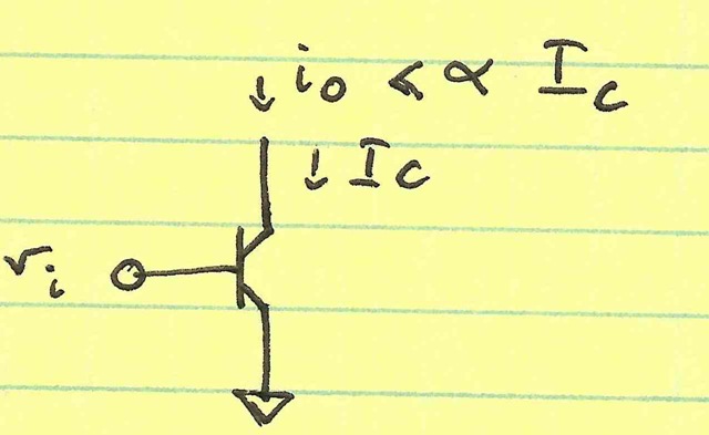
Pnoise = ×ばつk×ばつIC/Vt
Psig = ×ばつIC^2
SNR = ×ばつIC×ばつVt/(×ばつk×ばつB)
Once again, this IC×ばつVt is a lower-bound on the noise dissipated across the BJT: VBE > Vt and VCE > VBE → VCE > Vt. The true power dissipated across the BJT is IC×ばつVCE which is greater than Pmin = IC×ばつVt, and to maintain a certain SNR, we have Pmin = ×ばつk×ばつB/(α^2).
Loads
Resistor Noise
We now veer off into load country, considering resistor loads for our transconductor:
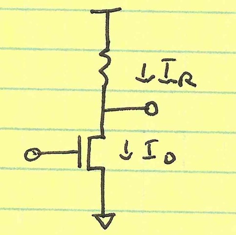
Considering only noise due to the resistor, and making the assumption that the signal current is once again limited to ×ばつID (where ID = IR):
Pnoise = ×ばつk×ばつB/R = ×ばつk×ばつIR/VR
SNR = ×ばつIR×ばつVR/(×ばつk&Times×ばつB)
Note that this case is not general: in many cases, we don’t have to have IR = ID, so the Psig has nothing to do with the resistor current. My intent is not to generalize to that much degree. I assume we have a transconductor–and every transconductor has to have a load (resistive, inductive, or active) that supplies dc current.
Active Loads
Going through the math, one finds that active loads (BJT or MOS) also follow a similar derivation: the noise contributed by the load is proportional to the current to minimum-voltage ratio of the load. Also, the signal current coming into the load is constrained by the load current, since that same load current flows through the transconductor:
MOS Load: Pnoise = ×ばつk×ばつID×ばつB/(×ばつVDSat) | Psig = ×ばつID
BJT Load: Pnoise = ×ばつk×ばつIC/Vt | Psig = ×ばつIC
Final Note
One final note: many times circuit designers think that they need to maximize gm of devices to minimize noise. This optimum is not always the case. Generally, for a transconductor, better gm yields better SNR (assuming linearity is not an issue). However, the gm of a load makes it add more (current) noise without improving signal power. Therefore, for loads, one wants to minimize gm.
[…] and are within the desired current limits. The power dissipated across the PMOS and NMOS devices which dictate SNR […]
This site uses Akismet to reduce spam. Learn how your comment data is processed.